参数资料
| 型号: | LTC6990IS6#TRPBF |
| 厂商: | Linear Technology |
| 文件页数: | 4/30页 |
| 文件大小: | 0K |
| 描述: | IC OSC SILICON 1MHZ TSOT23-6 |
| 产品培训模块: | TimerBlox Family Timing Devices |
| 特色产品: | TimerBlox? |
| 标准包装: | 2,500 |
| 系列: | TimerBlox® |
| 类型: | 振荡器 - 硅 |
| 频率: | 488Hz ~ 1MHz |
| 电源电压: | 2.25 V ~ 5.5 V |
| 电流 - 电源: | 235µA |
| 工作温度: | -40°C ~ 85°C |
| 封装/外壳: | SOT-23-6 细型,TSOT-23-6 |
| 包装: | 带卷 (TR) |
| 供应商设备封装: | TSOT-23-6 |
| 安装类型: | 表面贴装 |
| 配用: | DC1562A-A-ND - BOARD EVAL LTC6990 |
第1页第2页第3页当前第4页第5页第6页第7页第8页第9页第10页第11页第12页第13页第14页第15页第16页第17页第18页第19页第20页第21页第22页第23页第24页第25页第26页第27页第28页第29页第30页
LTC6990
12
6990fc
For more information www.linear.com/LTC6990
OPERATION
is not stable, it will increase the start-up time as the con-
verter waits for a stable result. Therefore, capacitance on
the DIV pin should be minimized so it will settle quickly.
Less than 100pF will not affect performance.
Output Enable
The OE pin controls the state of the LTC6990’s output as
seen on the OUT pin. Pulling the OE pin high enables the
oscillator output. Pulling it low disables the output. When
the output is disabled, it is either held low or placed in
a high impedance state as dictated by the Hi-Z bit value
(determined by the DIVCODE as described earlier). Table 2
summarizes the output control states.
Table 2. Output States
OE Pin
Hi-Z
OUT
1
X
Enabled, Output is Active
0
1
Disabled, Output is Hi-Z
0
Disabled, Output is Held Low
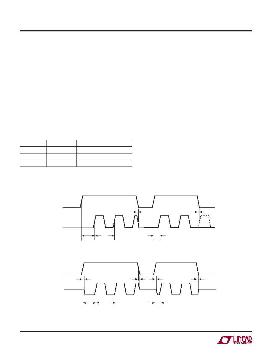
Figure 3 illustrates the timing for the OE function when
Hi-Z = 0. When OE is low, the output is disabled and OUT
is held low. Bringing OE high enables the output after a
delay, tENABLE, which synchronizes the enable to eliminate
sliver pulses and guarantee the correct width for the first
pulse. If NDIV = 1 or 2 this delay will be no longer than
the output period, tOUT. If NDIV > 2 the delay is limited to
twice the internal master oscillator period (or 2 tMASTER).
Forcing OE low will bring OUT low after a propagation
delay, tPD. If the output is high when OE falls, the output
pulse will be truncated.
As shown in Figure 4, setting Hi-Z = 1 places the output in
a high-impedance state when OE = 0. This feature allows
for“wired-OR”connectionsofmultipledevices.DrivingOE
high enables the output. The output will usually be forced
low during this time, although it is possible for OUT to
transition directly from high-impedance to a high output,
depending on the timing of the OE transition relative to
the internal oscillator. Once high, the first output pulse
will have the correct width (unless truncated by bringing
OE low again).
Figure 3. OE Timing Diagram (Hi-Z = 0)
6990 F03
OE
OUT
tPD
tENABLE
tOUT
Figure 4. OE Timing Diagram (Hi-Z = 1)
6990 F04
OE
OUT
tPD
tENABLE
tOUT
Hi-Z
相关PDF资料 |
PDF描述 |
|---|---|
| LTC6992HDCB-1#TRMPBF | IC OSC SILICON 1MHZ 6-DFN |
| LTC6990HDCB#TRMPBF | IC OSC SILICON 1MHZ 6DFN |
| V375B12M300BL | CONVERTER MOD DC/DC 12V 300W |
| V375B12M300BF3 | CONVERTER MOD DC/DC 12V 300W |
| V375A8M300BF2 | CONVERTER MOD DC/DC 8V 300W |
相关代理商/技术参数 |
参数描述 |
|---|---|
| LTC6990MPS6#PBF | 制造商:Linear Technology 功能描述:SC-Timing, Cut Tape VCO with Confirgurable Gain and Voltage Range, MP |
| LTC6990MPS6#TRMPBF | 功能描述:IC VCO CONFIG GAIN/VOLT TSOT23-6 RoHS:是 类别:集成电路 (IC) >> 时钟/计时 - 可编程计时器和振荡器 系列:TimerBlox® 产品培训模块:Lead (SnPb) Finish for COTS Obsolescence Mitigation Program 标准包装:45 系列:- 类型:温度 - 补偿晶体振荡器(TCXO) 计数:- 频率:25MHz 电源电压:3.135 V ~ 3.465 V 电流 - 电源:1.5mA 工作温度:-40°C ~ 85°C 封装/外壳:16-SOIC(0.295",7.50mm 宽) 包装:管件 供应商设备封装:16-SOIC W 安装类型:表面贴装 |
| LTC6990MPS6#TRPBF | 功能描述:IC VCO CONFIG GAIN/VOLT TSOT23-6 RoHS:是 类别:集成电路 (IC) >> 时钟/计时 - 可编程计时器和振荡器 系列:TimerBlox® 产品培训模块:Lead (SnPb) Finish for COTS Obsolescence Mitigation Program 标准包装:45 系列:- 类型:温度 - 补偿晶体振荡器(TCXO) 计数:- 频率:25MHz 电源电压:3.135 V ~ 3.465 V 电流 - 电源:1.5mA 工作温度:-40°C ~ 85°C 封装/外壳:16-SOIC(0.295",7.50mm 宽) 包装:管件 供应商设备封装:16-SOIC W 安装类型:表面贴装 |
| LTC6991 | 制造商:LINER 制造商全称:Linear Technology 功能描述:TimerBlox: Resettable, Low Frequency Oscillator |
| LTC6991CDCB#TRMPBF | 功能描述:IC OSC SILICON 977HZ 6-DFN RoHS:是 类别:集成电路 (IC) >> 时钟/计时 - 可编程计时器和振荡器 系列:TimerBlox® 标准包装:3,000 系列:- 类型:振荡器 - 晶体 计数:- 频率:- 电源电压:2.3 V ~ 5.5 V 电流 - 电源:1.07mA 工作温度:-30°C ~ 80°C 封装/外壳:SOT-665 包装:带卷 (TR) 供应商设备封装:SS迷你型-5D 安装类型:表面贴装 其它名称:AN8955SSMTXLTR |
发布紧急采购,3分钟左右您将得到回复。