- 您现在的位置:买卖IC网 > PDF目录9517 > LTC6992CDCB-4#TRMPBF (Linear Technology)IC OSC SILICON 1MHZ 6-DFN PDF资料下载
参数资料
| 型号: | LTC6992CDCB-4#TRMPBF |
| 厂商: | Linear Technology |
| 文件页数: | 4/34页 |
| 文件大小: | 0K |
| 描述: | IC OSC SILICON 1MHZ 6-DFN |
| 产品培训模块: | TimerBlox Family Timing Devices |
| 产品目录绘图: | LTC699_DFN |
| 特色产品: | LTC?6992 TimerBlox? TimerBlox? |
| 标准包装: | 1 |
| 系列: | TimerBlox® |
| 类型: | 振荡器 - 硅 |
| 频率: | 3.81Hz ~ 1MHz |
| 电源电压: | 2.25 V ~ 5.5 V |
| 电流 - 电源: | 365µA |
| 工作温度: | 0°C ~ 70°C |
| 封装/外壳: | 6-WFDFN 裸露焊盘 |
| 包装: | 标准包装 |
| 供应商设备封装: | 6-DFN-EP(2x3) |
| 安装类型: | 表面贴装 |
| 配用: | DC1562A-C-ND - BOARD EVAL LTC6992-1 |
| 其它名称: | LTC6992CDCB-4#TRMPBFDKR |
第1页第2页第3页当前第4页第5页第6页第7页第8页第9页第10页第11页第12页第13页第14页第15页第16页第17页第18页第19页第20页第21页第22页第23页第24页第25页第26页第27页第28页第29页第30页第31页第32页第33页第34页
LTC6992-1/LTC6992-2/
LTC6992-3/LTC6992-4
12
69921234fc
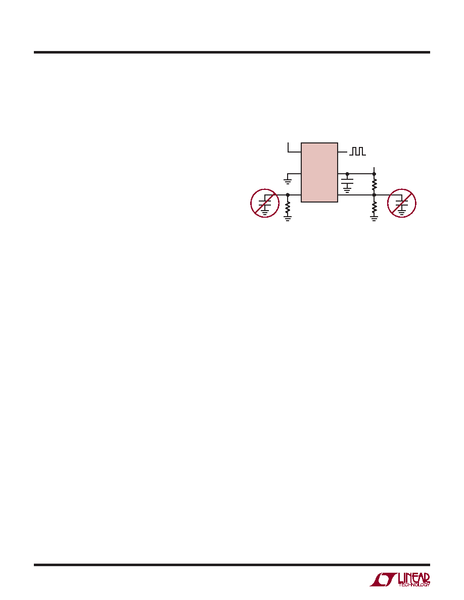
pin FuncTions
V+ (Pin 1/Pin 5): Supply Voltage (2.25V to 5.5V). This sup-
ply should be kept free from noise and ripple. It should be
bypassed directly to the GND pin with a 0.1μF capacitor.
DIV (Pin 2/Pin 4): Programmable Divider and Polarity
Input. The DIV pin voltage (VDIV) is internally converted
into a 4-bit result (DIVCODE). VDIV may be generated by
a resistor divider between V+ and GND. Use 1% resistors
to ensure an accurate result. The DIV pin and resistors
should be shielded from the OUT pin or any other traces
that have fast edges. Limit the capacitance on the DIV pin
to less than 100pF so that VDIV settles quickly. The MSB of
DIVCODE (POL) determines if the PWM signal is inverted
before driving the output. When POL = 1 the transfer func-
tion is inverted (duty cycle decreasing as VMODincreases).
SET (Pin 3/Pin 3): Frequency-Setting Input. The voltage
on the SET pin (VSET) is regulated to 1V above GND. The
amount of current sourced from the SET pin (ISET) pro-
grams the master oscillator frequency. The ISET current
range is 1.25μA to 20μA. The output oscillation will stop
if ISET drops below approximately 500nA. A resistor con-
nected between SET and GND is the most accurate way to
set the frequency. For best performance, use a precision
metal or thin film resistor of 0.5% or better tolerance and
50ppm/°C or better temperature coefficient. For lower ac-
curacy applications an inexpensive 1% thick film resistor
may be used.
Limit the capacitance on the SET pin to less than 10pF
to minimize jitter and ensure stability. Capacitance less
than 100pF maintains the stability of the feedback circuit
regulating the VSET voltage.
(DCB/S6)
6992 PF
LTC6992
MOD
GND
SET
OUT
V+
DIV
C1
0.1F
RSET
R2
R1
V+
MOD (Pin 4/Pin 1): Pulse-Width Modulation Input. The
voltage on the MOD pin controls the output duty cycle. The
linear control range is between 0.1 VSET and 0.9VSET
(approximately 100mV to 900mV). Beyond those limits,
the output will either clamp at 5% or 95%, or stop oscil-
lating (0% or 100% duty cycle), depending on the version.
GND (Pin 5/Pin 2): Ground. Tie to a low inductance ground
plane for best performance.
OUT (Pin 6/Pin 6): Oscillator Output. The OUT pin swings
fromGNDtoV+withanoutputresistanceofapproximately
30Ω. The duty cycle is determined by the voltage on the
MOD pin. When driving an LED or other low-impedance
load a series output resistor should be used to limit the
source/sink current to 20mA.
相关PDF资料 |
PDF描述 |
|---|---|
| VE-2TF-MY-S | CONVERTER MOD DC/DC 72V 50W |
| VI-B1D-IU-S | CONVERTER MOD DC/DC 85V 200W |
| VE-2T3-MY-S | CONVERTER MOD DC/DC 24V 50W |
| VI-B1B-IU-S | CONVERTER MOD DC/DC 95V 200W |
| VE-25Z-MY-S | CONVERTER MOD DC/DC 2V 20W |
相关代理商/技术参数 |
参数描述 |
|---|---|
| LTC6992CDCB6-1-PBF | 制造商:LINER 制造商全称:Linear Technology 功能描述:TimerBlox Voltage-Controlled Pulse Width Modulator (PWM) |
| LTC6992CDCB6-1-TRPBF | 制造商:LINER 制造商全称:Linear Technology 功能描述:TimerBlox Voltage-Controlled Pulse Width Modulator (PWM) |
| LTC6992CDCB6-2-PBF | 制造商:LINER 制造商全称:Linear Technology 功能描述:TimerBlox Voltage-Controlled Pulse Width Modulator (PWM) |
| LTC6992CDCB6-2-TRPBF | 制造商:LINER 制造商全称:Linear Technology 功能描述:TimerBlox Voltage-Controlled Pulse Width Modulator (PWM) |
| LTC6992CDCB6-3-PBF | 制造商:LINER 制造商全称:Linear Technology 功能描述:TimerBlox Voltage-Controlled Pulse Width Modulator (PWM) |
发布紧急采购,3分钟左右您将得到回复。