- 您现在的位置:买卖IC网 > PDF目录45000 > LTM8052IV#PBF (LINEAR TECHNOLOGY CORP) SWITCHING REGULATOR, 1000 kHz SWITCHING FREQ-MAX, PBGA81 PDF资料下载
参数资料
| 型号: | LTM8052IV#PBF |
| 厂商: | LINEAR TECHNOLOGY CORP |
| 元件分类: | 稳压器 |
| 英文描述: | SWITCHING REGULATOR, 1000 kHz SWITCHING FREQ-MAX, PBGA81 |
| 封装: | 15 X 11.25 MM, 2.82 MM HEIGHT, ROHS COMPLIANT, MO-222, LGA-81 |
| 文件页数: | 11/28页 |
| 文件大小: | 350K |
| 代理商: | LTM8052IV#PBF |
第1页第2页第3页第4页第5页第6页第7页第8页第9页第10页当前第11页第12页第13页第14页第15页第16页第17页第18页第19页第20页第21页第22页第23页第24页第25页第26页第27页第28页
LTM8052
19
8052f
applicaTions inForMaTion
No Output Current Sharing
The LTM8052 is a two quadrant device, able to both sink
and source current to maintain voltage regulation. It is
therefore not suitable for current sharing.
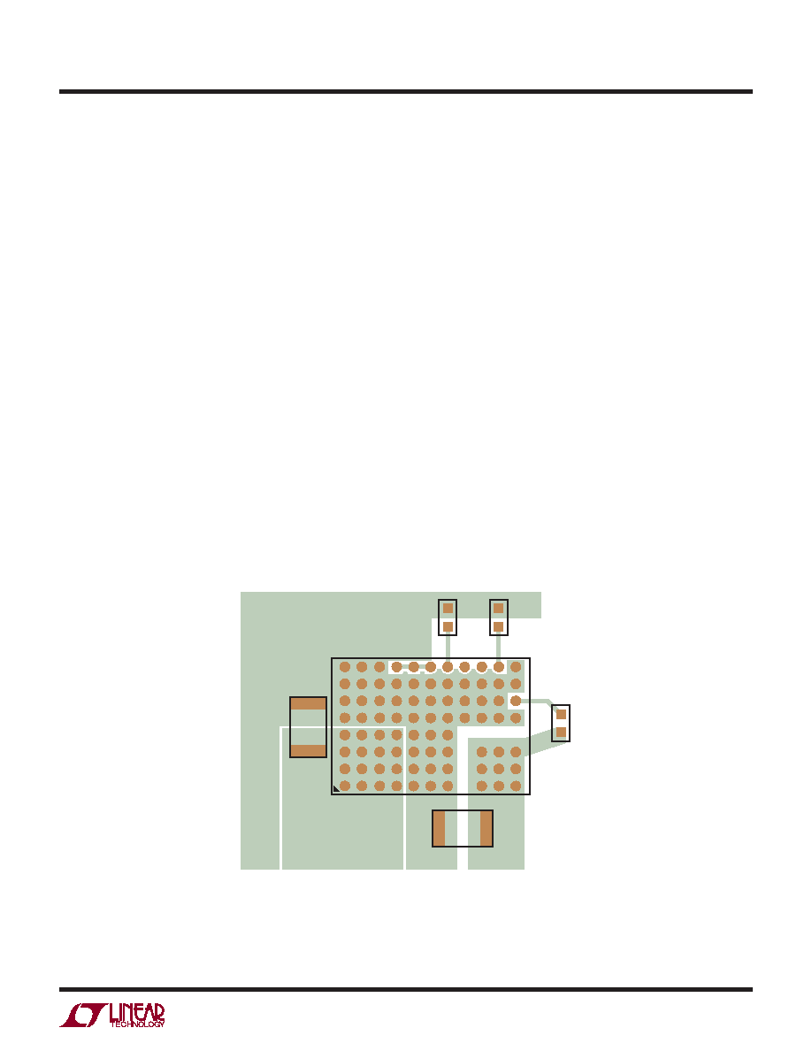
PCB Layout
Most of the headaches associated with PCB layout have
been alleviated or even eliminated by the high level of
integration of the LTM8052. The LTM8052 is neverthe-
less a switching power supply, and care must be taken to
minimize EMI and ensure proper operation. Even with the
high level of integration, you may fail to achieve specified
operation with a haphazard or poor layout. See Figure 6
for a suggested layout. Ensure that the grounding and
heat sinking are acceptable.
A few rules to keep in mind are:
1. Place the RADJ and RT resistors as close as possible to
their respective pins.
2. Place the CIN capacitor as close as possible to the VIN
and GND connection of the LTM8052.
CTL_T
CTL_I
V REF
COMP
SS
ADJ
SYNC
VIN
VIN
8052 F06
GND
CIN
VOUT
COUT
GND
THERMAL AND INTERCONNECT VIAS
RUN
RT
3. Place the COUT capacitor as close as possible to the
VOUT and GND connection of the LTM8052.
4. Place the CIN and COUT capacitors such that their
ground currents flow directly adjacent or underneath
the LTM8052.
5. Connect all of the GND connections to as large a copper
pour or plane area as possible on the top layer. Avoid
breaking the ground connection between the external
components and the LTM8052.
6. Use vias to connect the GND copper area to the board’s
internal ground planes. Liberally distribute these GND
vias to provide both a good ground connection and
thermal path to the internal planes of the printed circuit
board. Pay attention to the location and density of the
thermal vias in Figure 6. The LTM8052 can benefit from
the heat sinking afforded by vias that connect to internal
GND planes at these locations, due to their proximity
to internal power handling components. The optimum
number of thermal vias depends upon the printed
circuit board design. For example, a board might use
very small via holes. It should employ more thermal
vias than a board that uses larger holes.
Figure 6. Layout Showing Suggested External Components,
GND Plane and Thermal Vias.
相关PDF资料 |
PDF描述 |
|---|---|
| LTM8062EV#PBF | BATTERY CHARGE CONTROLLER, 1150 kHz SWITCHING FREQ-MAX, PBGA77 |
| LTM8062AEV#PBF | BATTERY CHARGE CONTROLLER, 1150 kHz SWITCHING FREQ-MAX, PBGA77 |
| LTM9005CV-AA#PBF | SPECIALTY ANALOG CIRCUIT, PBGA204 |
| LTM9005CV-AB#PBF | SPECIALTY ANALOG CIRCUIT, PBGA204 |
| LTM9005IV-AB#PBF | SPECIALTY ANALOG CIRCUIT, PBGA204 |
相关代理商/技术参数 |
参数描述 |
|---|---|
| LTM8061 | 制造商:LINER 制造商全称:Linear Technology 功能描述:32V, 2A μModule Li-Ion/ Polymer Battery Charger |
| LTM8061EV-4.1#PBF | 功能描述:IC BATTERY CHARGER 4.1V 77-LGA RoHS:是 类别:集成电路 (IC) >> PMIC - 电池管理 系列:µModule® 其它有关文件:STC3100 View All Specifications 特色产品:STC3100 - Battery Monitor IC 标准包装:4,000 系列:- 功能:燃料,电量检测计/监控器 电池化学:锂离子(Li-Ion) 电源电压:2.7 V ~ 5.5 V 工作温度:-40°C ~ 85°C 安装类型:表面贴装 封装/外壳:8-TSSOP,8-MSOP(0.118",3.00mm 宽) 供应商设备封装:8-MiniSO 包装:带卷 (TR) 其它名称:497-10526-2 |
| LTM8061EV-4.1PBF | 制造商:LINER 制造商全称:Linear Technology 功能描述:32V, 2A μModule Li-Ion/ Polymer Battery Charger |
| LTM8061EV-4.2#PBF | 功能描述:IC BATTERY CHARGER 4.2V 77-LGA RoHS:是 类别:集成电路 (IC) >> PMIC - 电池管理 系列:µModule® 其它有关文件:STC3100 View All Specifications 特色产品:STC3100 - Battery Monitor IC 标准包装:4,000 系列:- 功能:燃料,电量检测计/监控器 电池化学:锂离子(Li-Ion) 电源电压:2.7 V ~ 5.5 V 工作温度:-40°C ~ 85°C 安装类型:表面贴装 封装/外壳:8-TSSOP,8-MSOP(0.118",3.00mm 宽) 供应商设备封装:8-MiniSO 包装:带卷 (TR) 其它名称:497-10526-2 |
| LTM8061EV-4.2PBF | 制造商:LINER 制造商全称:Linear Technology 功能描述:32V, 2A μModule Li-Ion/ Polymer Battery Charger |
发布紧急采购,3分钟左右您将得到回复。