- 您现在的位置:买卖IC网 > PDF目录45008 > LX1684CD-TR (MICROSEMI CORP-ANALOG MIXED SIGNAL GROUP) 1 A SWITCHING CONTROLLER, 200 kHz SWITCHING FREQ-MAX, PDSO14 PDF资料下载
参数资料
| 型号: | LX1684CD-TR |
| 厂商: | MICROSEMI CORP-ANALOG MIXED SIGNAL GROUP |
| 元件分类: | 稳压器 |
| 英文描述: | 1 A SWITCHING CONTROLLER, 200 kHz SWITCHING FREQ-MAX, PDSO14 |
| 封装: | PLASTIC, SOIC-14 |
| 文件页数: | 10/12页 |
| 文件大小: | 248K |
| 代理商: | LX1684CD-TR |
Microsemi
Integrated Products Division
11861 Western Avenue, Garden Grove, CA. 92841, 714-898-8121, Fax: 714-893-2570
Page 7
Copyright
2000
Rev. 1.0c, 2005-03-08
WWW
.Microse
m
i
.CO
M
LX1684
Voltage-Mode PWM Controller
PRODUCTION DATA SHEET
TM
APPLI CATI ON I N FORMATI O N
SOFT-START CAPACITOR (continued)
The capacitor current to follow the SS-pin voltage is:
()
SS
OUT
C
R
t
SS
OUT
C
e
C
dt
dV
C
I
/
×
=
where COUT is the output capacitance. The typical value of CSS
should be in the range of 0.1 to 0.2F.
During the soft-start interval the load current from a
microprocessor is negligible; therefore, the capacitor current is
approximately the required inductor current.
OVER-CURRENT PROTECTION
Current limiting occurs at current level ICL , when the voltage
detected by the current sense comparator is greater than the current
sense comparator threshold, VTRIP (400mV).
TRIP
SET
ON
DS
CL
V
R
I
R
I
=
×
+
×
)
(
So,
A
R
I
mV
R
I
R
I
V
R
ON
DS
CL
SET
ON
DS
CL
TRIP
SET
45
400
)
(
)
(
×
=
×
=
Example:
For 10A current limit, using SUB45N05-20L MOSFET (20m
RDS(ON) ):
=
×
=
k
RSET
42
4
10
45
020
0
10
4
0
6
.
Current Sensing Using Sense Resistor
The method of current sensing using the RDS(ON) of the upper
MOSFET is economical, but can have a large tolerance, since the
RDS(ON) can vary with temperature, etc. A more accurate alternative
is to use an external sense resistor (RSENSE ). The sense resistor
could be a PCB trace (for construction details, see Application
Note AN-10 or LX1668 data sheet). The over-current trip point is
calculated as in the equations above, replacing RDS(ON) with RSENSE .
Example:
For 10A current limit, using a 5m sense resistor:
=
×
=
×
=
k
R
I
R
I
V
R
SET
SENSE
CL
TRIP
SET
8
.
7
10
45
005
.
0
10
4
.
0
)
(
6
OUTPUT ENABLE
The LX1684 FET driver outputs are driven to ground by pulling
the soft-start pin below 0.3V.
PROGRAMMING THE OUTPUT VOLTAGE
The output voltage is sensed by the feedback pin (V FB ) which
has a 1.25V reference. The output voltage can be set to any voltage
above 1.25V (and lower than the input voltage) by means of a
resistor divider (see Product Highlight).
)
1
(
2
1
R
V
REF
OUT
+
=
Note: Keep R 1 and R 2 close to 100
(order of magnitude).
FET SELECTION
To insure reliable operation, the operating junction temperature
of the FET switches must be kept below certain limits. The Intel
specification states that 115°C maximum junction temperature
should be maintained with an ambient of 50°C. This is achieved by
properly derating the part, and by adequate heat sinking. One of the
most critical parameters for FET selection is the RDS(ON) resistance.
This parameter directly contributes to the power dissipation of the
FET devices, and thus impacts heat sink design, mechanical layout,
and reliability. In general, the larger the current handling capability
of the FET, the lower the R DS(ON) will be, since more die area is
available.
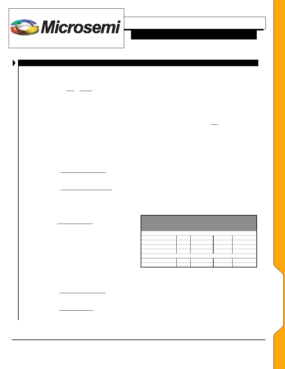
TABLE 1 - FET Selection Guide
This table gives selection of suitable FETs from VISHAY
Device
VDS
(V)
RDS(ON)
@4.5V
(m)
RDS(ON)
@10V
(m)
Gate
Charge
typ(nC)
D
2PAK and TO-220
SUB70N03-09BP
30
13
9
15.5
SUB45N03-13L
30
20
13
45
SUB45N05-20L
40
20
18
43
SUB70N04-10
40
14
10
50
SO-8
Si4810DY
30
20
13.5
20
Si4812DY
30
28
18
16
Heat Dissipated In Upper MOSFET
The heat dissipated in the top MOSFET will be:
)
5
.
0
(
)
(
)
(
2
S
SW
IN
ON
DS
D
f
t
V
I
Cycle
Duty
R
I
P
×
+
×
=
Where tSW is switching transition line for body diode (~100ns) and
fS is the switching frequency.
For the SUB70N03-09BP (13m RDS(ON) ), converting 12V to
3.3V at 15A will result in typical heat dissipation of 2.6W.
AA
PP
LL
IICC
AA
TT
IIOO
NN
SS
相关PDF资料 |
PDF描述 |
|---|---|
| LX1688IPW-TR | FLUORESCENT LIGHT CONTROLLER, 70 kHz SWITCHING FREQ-MAX, PDSO24 |
| LX1689IPWT | FLUORESCENT LIGHT CONTROLLER, 500 kHz SWITCHING FREQ-MAX, PDSO20 |
| LX1689CPWT | FLUORESCENT LIGHT CONTROLLER, 500 kHz SWITCHING FREQ-MAX, PDSO20 |
| LX1691AIPW-TR | 0.1 A FLUORESCENT LIGHT CONTROLLER, 250 kHz SWITCHING FREQ-MAX, PDSO16 |
| LX1692BIPW-TR | 0.1 A SWITCHING CONTROLLER, PDSO20 |
相关代理商/技术参数 |
参数描述 |
|---|---|
| LX1686 | 制造商:MICROSEMI 制造商全称:Microsemi Corporation 功能描述:Digital Dimming CCFL Controller IC |
| LX1686CPW | 功能描述:IC CTRLR CCFL BACKLIGHT 24TSSOP RoHS:是 类别:集成电路 (IC) >> PMIC - 照明,镇流器控制器 系列:- 产品培训模块:Lead (SnPb) Finish for COTS Obsolescence Mitigation Program 标准包装:2,500 系列:- 类型:CCFL 控制器 频率:40 ~ 80 kHz 电流 - 电源:5mA 电流 - 输出:- 电源电压:4.5 V ~ 5.5 V 工作温度:-40°C ~ 85°C 封装/外壳:16-SOIC(0.154",3.90mm 宽) 供应商设备封装:16-SOIC 包装:带卷 (TR) 其它名称:90-3991V+V01 |
| LX1686CPWT | 制造商:未知厂家 制造商全称:未知厂家 功能描述:Ballast/Backlight Controller/Driver |
| LX1686CPW-TR | 制造商:Microsemi Corporation 功能描述:CCFL Controller 3.3V/5V 24-Pin TSSOP T/R |
| LX1686E | 制造商:MICROSEMI 制造商全称:Microsemi Corporation 功能描述:Digital Dimming CCFL Controller IC |
发布紧急采购,3分钟左右您将得到回复。