- 您现在的位置:买卖IC网 > PDF目录45008 > LX1684CD-TR (MICROSEMI CORP-ANALOG MIXED SIGNAL GROUP) 1 A SWITCHING CONTROLLER, 200 kHz SWITCHING FREQ-MAX, PDSO14 PDF资料下载
参数资料
| 型号: | LX1684CD-TR |
| 厂商: | MICROSEMI CORP-ANALOG MIXED SIGNAL GROUP |
| 元件分类: | 稳压器 |
| 英文描述: | 1 A SWITCHING CONTROLLER, 200 kHz SWITCHING FREQ-MAX, PDSO14 |
| 封装: | PLASTIC, SOIC-14 |
| 文件页数: | 11/12页 |
| 文件大小: | 248K |
| 代理商: | LX1684CD-TR |
Microsemi
Integrated Products Division
11861 Western Avenue, Garden Grove, CA. 92841, 714-898-8121, Fax: 714-893-2570
Page 8
Copyright
2000
Rev. 1.0c, 2005-03-08
WWW
.Microse
m
i
.CO
M
LX1684
Voltage-Mode PWM Controller
PRODUCTION DATA SHEET
TM
APPLI CATI ON I N FORMATI O N
FET SELECTION (continued)
Synchronous Rectification – Lower MOSFET
The lower pass element can be either a MOSFET or a Schottky
diode. The use of a MOSFET (synchronous rectification) will
result in higher efficiency, but at higher cost than using a Schottky
diode (non-synchronous). Power dissipated in the bottom
MOSFET will be:
[]
W
Cycle
Duty
R
I
P
ON
DS
D
26
3
1
2
.
)
(
=
×
=
[SUB45N03-13L or 2.12W for the SUB70N03-09BP]
Non-Synchronous Operation - Schottky Diode
A typical Schottky diode, with a forward drop of 0.6V will
dissipate 0.6 * 15 * [1 – 3.3/12] = 6.5W (compared to the 2.1 to
4.2W dissipated by a MOSFET under the same conditions). This
power loss becomes much more significant at lower duty cycles.
The use of a dual Schottky diode in a single TO-220 package (e.g.
the MBR2535) helps improve thermal dissipation.
Boost Operation
The LX1684 needs a secondary supply voltage (VC1) to provide
sufficient drive to the upper MOSFET. The top FET must be a
logic level power MOSFET such as SUB45N03-13L. It must be able
to turn on to a low RDS(ON) with VGS of 4.5V or higher. VC1 can be
generated using a bootstrap (charge pump) circuit, as shown in the
Product Highlight on page 1. The capacitor, (C1) is alternatively
charged up from 5V via the Schottky diode, (D1), and then boosted
up when the FET is turned on. Under any circumstance the voltage
at VC1 should not be more than 18V for more than 300nS and must
not be greater than 19V for more than 50nS. Lab evaluation and
module production test should be the final arbiter to verify the
proper operation. For application with a large MOSFET, the
maximum voltage at VC1 should be kept lower due to thermal
dissipation in the FET driver section. It is inherent in a higher
current power supply that the parasitic inductance and capacitance
on PCB board and Power MOSFET device induces ringing at the
gate drive. The extra thermal dissipation and the higher peak
voltage generated by gate ringing should be taken in account
during final design. The temperature rise due to gate drive thermal
dissipation can be reduced by extra heat sinking. A resistor in
series with the gate in order of 10ohm or snubber circuitry can
reduce the gate ringing. The voltage must provide sufficient gate
drive to the external MOSFET in order to get a low RDS(ON) and
MUST be lower than maximum voltage rating of 18V.
Note that using the bootstrap circuit in synchronous rectification
mode is likely to result in faster turn-on than in non-synchronous
mode.
LAYOUT GUIDELINES - THERMAL DESIGN
A great deal of time and effort were spent optimizing the
thermal design of the demonstration boards. Any user who intends
to implement an embedded motherboard would be well advised to
carefully read and follow these guidelines.
If the FET switches have been carefully selected, external
heatsinking is generally not required. However, this means that
copper trace on the PC board must now be used. This is a potential
trouble spot; as much copper area as possible must be dedicated to
heatsinking the FET switches, and the diode as well if a non-
synchronous solution is used..
LX1684
+12V Input
O utput
GND
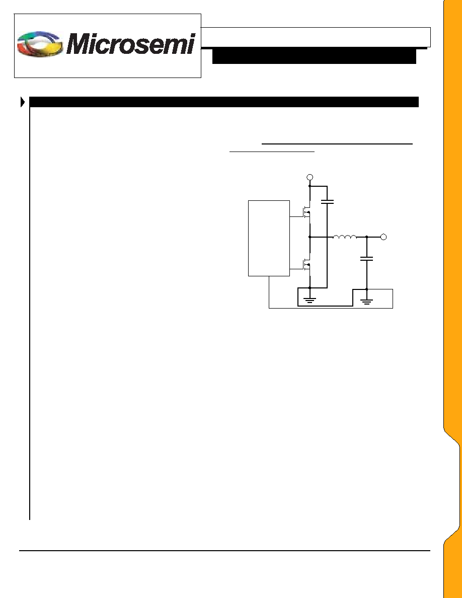
FIGURE 2 — Key Power PCB Traces
General Notes
As always, be sure to provide local capacitive decoupling close
to the chip. Be sure use ground plane construction for all high-
frequency work. Use low ESR capacitors where justified, but be
alert for damping and ringing problems. High-frequency designs
demand careful routing and layout, and may require several
iterations to achieve desired performance levels.
Power Traces
To reduce power losses due to ohmic resistance, careful consid-
eration should be given to the layout of traces that carry high
currents. The main paths to consider are:
Input power from 12V supply to drain of top MOSFET.
Trace between top MOSFET and lower MOSFET or
Schottky diode.
Trace between lower MOSFET or Schottky diode and
ground.
Trace between source of top MOSFET and inductor and
load.
All of these traces should be made as wide and thick as possible,
in order to minimize resistance and hence power losses. It is also
recommended that, whenever possible, the ground, input and
output power signals should be on separate planes (PCB layers).
See Figure 2 – bold traces are power traces.
AA
PP
LL
IICC
AA
TT
IIOO
NN
SS
相关PDF资料 |
PDF描述 |
|---|---|
| LX1688IPW-TR | FLUORESCENT LIGHT CONTROLLER, 70 kHz SWITCHING FREQ-MAX, PDSO24 |
| LX1689IPWT | FLUORESCENT LIGHT CONTROLLER, 500 kHz SWITCHING FREQ-MAX, PDSO20 |
| LX1689CPWT | FLUORESCENT LIGHT CONTROLLER, 500 kHz SWITCHING FREQ-MAX, PDSO20 |
| LX1691AIPW-TR | 0.1 A FLUORESCENT LIGHT CONTROLLER, 250 kHz SWITCHING FREQ-MAX, PDSO16 |
| LX1692BIPW-TR | 0.1 A SWITCHING CONTROLLER, PDSO20 |
相关代理商/技术参数 |
参数描述 |
|---|---|
| LX1686 | 制造商:MICROSEMI 制造商全称:Microsemi Corporation 功能描述:Digital Dimming CCFL Controller IC |
| LX1686CPW | 功能描述:IC CTRLR CCFL BACKLIGHT 24TSSOP RoHS:是 类别:集成电路 (IC) >> PMIC - 照明,镇流器控制器 系列:- 产品培训模块:Lead (SnPb) Finish for COTS Obsolescence Mitigation Program 标准包装:2,500 系列:- 类型:CCFL 控制器 频率:40 ~ 80 kHz 电流 - 电源:5mA 电流 - 输出:- 电源电压:4.5 V ~ 5.5 V 工作温度:-40°C ~ 85°C 封装/外壳:16-SOIC(0.154",3.90mm 宽) 供应商设备封装:16-SOIC 包装:带卷 (TR) 其它名称:90-3991V+V01 |
| LX1686CPWT | 制造商:未知厂家 制造商全称:未知厂家 功能描述:Ballast/Backlight Controller/Driver |
| LX1686CPW-TR | 制造商:Microsemi Corporation 功能描述:CCFL Controller 3.3V/5V 24-Pin TSSOP T/R |
| LX1686E | 制造商:MICROSEMI 制造商全称:Microsemi Corporation 功能描述:Digital Dimming CCFL Controller IC |
发布紧急采购,3分钟左右您将得到回复。