参数资料
| 型号: | M1A3P1000-FGG144I |
| 厂商: | Microsemi SoC |
| 文件页数: | 11/12页 |
| 文件大小: | 0K |
| 描述: | IC FPGA M1 1KB FLASH 1M 144FPGA |
| 标准包装: | 160 |
| 系列: | ProASIC3 |
| RAM 位总计: | 147456 |
| 输入/输出数: | 97 |
| 门数: | 1000000 |
| 电源电压: | 1.425 V ~ 1.575 V |
| 安装类型: | 表面贴装 |
| 工作温度: | -40°C ~ 85°C |
| 封装/外壳: | 144-LBGA |
| 供应商设备封装: | 144-FPBGA(13x13) |
ARM CortexTM-M1
8P ro d u c t B r i e f
Exception Priority
In the processor exception model, priority determines
when and how the processor takes exceptions. You can
assign software priority levels to interrupts.
The NVIC supports software-assigned priority levels. You
can assign a priority level from 0 to 3 to an interrupt by
writing to the 2-bit IP_N field in an Interrupt Priority
Register. Hardware priority decreases with increasing
interrupt number. Priority level –3 is the highest priority
level, and priority level 3 is the lowest. The priority level
overrides the hardware priority.
Stacks
The processor supports two separate stacks:
Process stack – You can configure Thread mode
to use the process stack. Thread mode uses the
main stack out of reset. SP_process is the Stack
Pointer (SP) register for the process stack.
Main stack – Handler mode uses the main stack.
SP_main is the SP register for the main stack.
Only one stack, the process stack or the main stack, is
visible at any time, using R13. After pushing the content,
the ISR uses the main stack, and all subsequent interrupt
preemptions use the main stack.
Clocking and Resets
The processor has one functional clock input, HCLK, and
one reset signal, SYSRESETn. If debug is implemented,
there is also a SWJ-DP clock, SWCLKTCK, and nTRST.
SWCLKTCK relates to the DAP logic. The debug reset
signal DBGRESETn relates to the debug logic clocked by
HCLK.
The SYSRESETn signal resets the entire processor system
with the exception of debug logic in the following:
Nested Vectored Interrupt Controller (NVIC)
Debug subsystem
The register file cannot be reset by SYSRESETn or
DBGRESETn.
Nested Vectored Interrupt Controller
The NVIC facilitates low-latency exception and interrupt
handling, and implements System Control Registers. The
NVIC supports reprioritizable interrupts. The NVIC and
the processor core interface are closely coupled, which
enables low latency interrupt processing and efficient
processing of late-arriving interrupts. All NVIC registers
are only accessible using word transfers. Any attempt to
write a halfword or byte individually causes corruption
of the register bits. All NVIC registers and system debug
registers are little-endian, regardless of the endianness
state of the processor. See Table 4 for a list of the NVIC
registers and their addresses
.
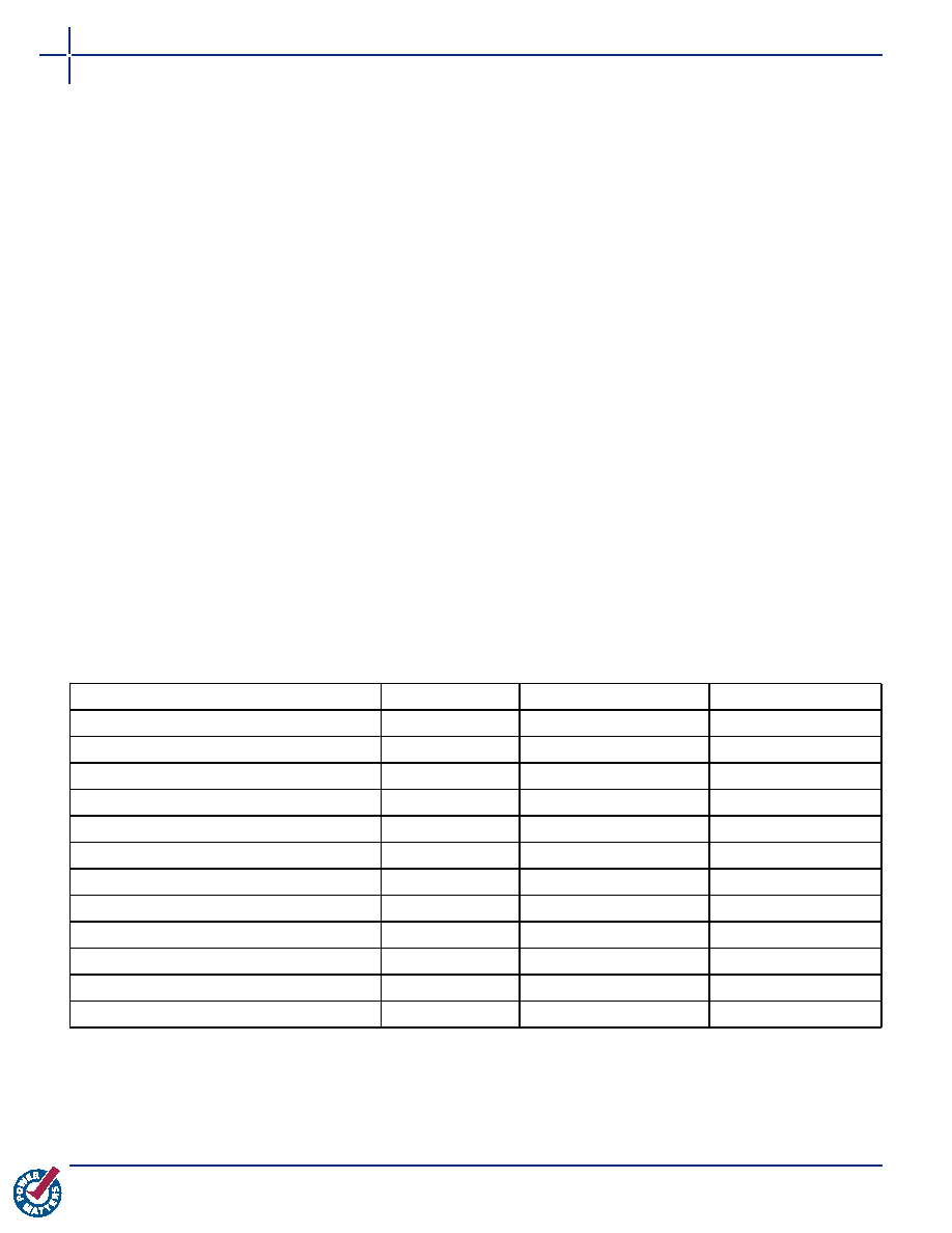
Table 4
NVIC Register
Name of Register
Type
Address
Reset Value
IRQ 0 to 31 Set Enable Register
R/W
0xE000E100
0x00000000
IRQ 0 to 31 Clear Enable Register
R/W
0xE000E180
0x00000000
IRQ 0 to 31 Set Pending Register
R/W
0xE000E200
0x00000000
IRQ 0 to 31 Clear Pending Register
R/W
0xE000E280
0x00000000
Priority 0 Register
R/W
0xE000E400
0x00000000
Priority 1 Register
R/W
0xe000e404
0x00000000
Priority 2 Register
R/W
0xe000e408
0x00000000
Priority 3 Register
R/W
0xe000e40c
0x00000000
Priority 4 Register
R/W
0xe000e410
0x00000000
Priority 5 Register
R/W
0xe000e414
0x00000000
Priority 6 Register
R/W
0xe000e418
0x00000000
Priority 7 Register
R/W
0xe000e41c
0x00000000
相关PDF资料 |
PDF描述 |
|---|---|
| A3P1000-FGG144I | IC FPGA 1KB FLASH 1M 144-FBGA |
| RMM36DTAD | CONN EDGECARD 72POS R/A .156 SLD |
| A54SX32A-TQG144A | IC FPGA SX 48K GATES 144-TQFP |
| A3PE600-1FGG256I | IC FPGA 600000 GATES 256-FBGA |
| ASM36DRYI | CONN EDGECARD 72POS DIP .156 SLD |
相关代理商/技术参数 |
参数描述 |
|---|---|
| M1A3P1000-FGG144M | 制造商:Microsemi Corporation 功能描述:FPGA PROASIC?3 FAMILY 1M GATES 130NM (CMOS) TECHNOLOGY 1.5V - Trays 制造商:Microsemi Corporation 功能描述:IC FPGA 1M GATES W/M1 144GBGA 制造商:Microsemi Corporation 功能描述:IC FPGA 97 I/O 144GBGA |
| M1A3P1000-FGG144PP | 制造商:ACTEL 制造商全称:Actel Corporation 功能描述:ProASIC3 Flash Family FPGAs |
| M1A3P1000-FGG256 | 功能描述:IC FPGA M1 1KB FLASH 1M 256FBGA RoHS:是 类别:集成电路 (IC) >> 嵌入式 - FPGA(现场可编程门阵列) 系列:ProASIC3 标准包装:90 系列:ProASIC3 LAB/CLB数:- 逻辑元件/单元数:- RAM 位总计:36864 输入/输出数:157 门数:250000 电源电压:1.425 V ~ 1.575 V 安装类型:表面贴装 工作温度:-40°C ~ 125°C 封装/外壳:256-LBGA 供应商设备封装:256-FPBGA(17x17) |
| M1A3P1000-FGG256I | 功能描述:IC FPGA M1 1KB FLASH 1M 256FBGA RoHS:是 类别:集成电路 (IC) >> 嵌入式 - FPGA(现场可编程门阵列) 系列:ProASIC3 标准包装:40 系列:SX-A LAB/CLB数:6036 逻辑元件/单元数:- RAM 位总计:- 输入/输出数:360 门数:108000 电源电压:2.25 V ~ 5.25 V 安装类型:表面贴装 工作温度:0°C ~ 70°C 封装/外壳:484-BGA 供应商设备封装:484-FPBGA(27X27) |
| M1A3P1000-FGG484 | 功能描述:IC FPGA M1 1KB FLASH 1M 484FBGA RoHS:是 类别:集成电路 (IC) >> 嵌入式 - FPGA(现场可编程门阵列) 系列:ProASIC3 标准包装:90 系列:ProASIC3 LAB/CLB数:- 逻辑元件/单元数:- RAM 位总计:36864 输入/输出数:157 门数:250000 电源电压:1.425 V ~ 1.575 V 安装类型:表面贴装 工作温度:-40°C ~ 125°C 封装/外壳:256-LBGA 供应商设备封装:256-FPBGA(17x17) |
发布紧急采购,3分钟左右您将得到回复。