- 您现在的位置:买卖IC网 > PDF目录224123 > M25P32VMN6G (意法半导体) 4 Mbit Uniform Sector, Serial Flash Memory PDF资料下载
参数资料
| 型号: | M25P32VMN6G |
| 厂商: | 意法半导体 |
| 元件分类: | FLASH |
| 英文描述: | 4 Mbit Uniform Sector, Serial Flash Memory |
| 中文描述: | 4兆位统一部门,串行闪存 |
| 文件页数: | 10/39页 |
| 文件大小: | 506K |
| 代理商: | M25P32VMN6G |
第1页第2页第3页第4页第5页第6页第7页第8页第9页当前第10页第11页第12页第13页第14页第15页第16页第17页第18页第19页第20页第21页第22页第23页第24页第25页第26页第27页第28页第29页第30页第31页第32页第33页第34页第35页第36页第37页第38页第39页
M25P32
18/39
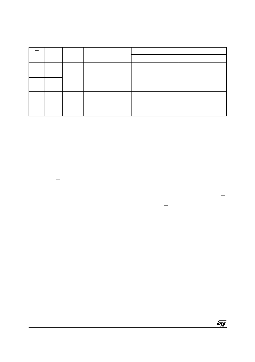
Table 7. Protection Modes
Note: 1. As defined by the values in the Block Protect (BP2, BP1, BP0) bits of the Status Register, as shown in Table 2..
The protection features of the device are summa-
rized in Table 7..
When the Status Register Write Disable (SRWD)
bit of the Status Register is 0 (its initial delivery
state), it is possible to write to the Status Register
provided that the Write Enable Latch (WEL) bit has
previously been set by a Write Enable (WREN) in-
struction, regardless of the whether Write Protect
(W) is driven High or Low.
When the Status Register Write Disable (SRWD)
bit of the Status Register is set to 1, two cases
need to be considered, depending on the state of
Write Protect (W):
–
If Write Protect (W) is driven High, it is
possible to write to the Status Register
provided that the Write Enable Latch (WEL) bit
has previously been set by a Write Enable
(WREN) instruction.
–
If Write Protect (W) is driven Low, it is not
possible to write to the Status Register even if
the Write Enable Latch (WEL) bit has
previously been set by a Write Enable
(WREN) instruction. (Attempts to write to the
Status Register are rejected, and are not
accepted for execution). As a consequence,
all the data bytes in the memory area that are
software protected (SPM) by the Block Protect
(BP2, BP1, BP0) bits of the Status Register,
are also hardware protected against data
modification.
Regardless of the order of the two events, the
Hardware Protected Mode (HPM) can be entered:
–
by setting the Status Register Write Disable
(SRWD) bit after driving Write Protect (W) Low
–
or by driving Write Protect (W) Low after
setting the Status Register Write Disable
(SRWD) bit.
The only way to exit the Hardware Protected Mode
(HPM) once entered is to pull Write Protect (W)
High.
If Write Protect (W) is permanently tied High, the
Hardware Protected Mode (HPM) can never be
activated, and only the Software Protected Mode
(SPM), using the Block Protect (BP2, BP1, BP0)
bits of the Status Register, can be used.
W
Signal
SRWD
Bit
Mode
Write Protection of the
Status Register
Memory Content
Protected Area1
Unprotected Area1
10
Software
Protected
(SPM)
Status Register is Writable
(if the WREN instruction
has set the WEL bit)
The values in the SRWD,
BP2, BP1 and BP0 bits
can be changed
Protected against Page
Program, Sector Erase
and Bulk Erase
Ready to accept Page
Program and Sector Erase
instructions
00
11
01
Hardware
Protected
(HPM)
Status Register is
Hardware write protected
The values in the SRWD,
BP2, BP1 and BP0 bits
cannot be changed
Protected against Page
Program, Sector Erase
and Bulk Erase
Ready to accept Page
Program and Sector Erase
instructions
相关PDF资料 |
PDF描述 |
|---|---|
| M25P32VMN6P | 4 Mbit Uniform Sector, Serial Flash Memory |
| M25P32VMN6T | 4 Mbit Uniform Sector, Serial Flash Memory |
| M25P32VMN6TG | 4 Mbit Uniform Sector, Serial Flash Memory |
| M25P32VMN6TP | 4 Mbit Uniform Sector, Serial Flash Memory |
| M25P32VMP3 | 4 Mbit Uniform Sector, Serial Flash Memory |
相关代理商/技术参数 |
参数描述 |
|---|---|
| M25P32VMN6P | 制造商:STMICROELECTRONICS 制造商全称:STMicroelectronics 功能描述:512 Kbit to 32 Mbit, Low Voltage, Serial Flash Memory With 40 MHz or 50 MHz SPI Bus Interface |
| M25P32VMN6T | 制造商:STMICROELECTRONICS 制造商全称:STMicroelectronics 功能描述:512 Kbit to 32 Mbit, Low Voltage, Serial Flash Memory With 40 MHz or 50 MHz SPI Bus Interface |
| M25P32VMN6TG | 制造商:STMICROELECTRONICS 制造商全称:STMicroelectronics 功能描述:512 Kbit to 32 Mbit, Low Voltage, Serial Flash Memory With 40 MHz or 50 MHz SPI Bus Interface |
| M25P32VMN6TP | 制造商:STMICROELECTRONICS 制造商全称:STMicroelectronics 功能描述:512 Kbit to 32 Mbit, Low Voltage, Serial Flash Memory With 40 MHz or 50 MHz SPI Bus Interface |
| M25P32VMP3 | 制造商:STMICROELECTRONICS 制造商全称:STMicroelectronics 功能描述:512 Kbit to 32 Mbit, Low Voltage, Serial Flash Memory With 40 MHz or 50 MHz SPI Bus Interface |
发布紧急采购,3分钟左右您将得到回复。