- 您现在的位置:买卖IC网 > PDF目录180109 > M27V256-100B6TR (意法半导体) 256 Kbit 32Kb x 8 Low Voltage UV EPROM and OTP EPROM PDF资料下载
参数资料
| 型号: | M27V256-100B6TR |
| 厂商: | 意法半导体 |
| 英文描述: | 256 Kbit 32Kb x 8 Low Voltage UV EPROM and OTP EPROM |
| 中文描述: | 256千位的32KB × 8低压紫外线可擦写可编程只读存储器和OTP存储器 |
| 文件页数: | 11/15页 |
| 文件大小: | 103K |
| 代理商: | M27V256-100B6TR |
5/15
M27V256
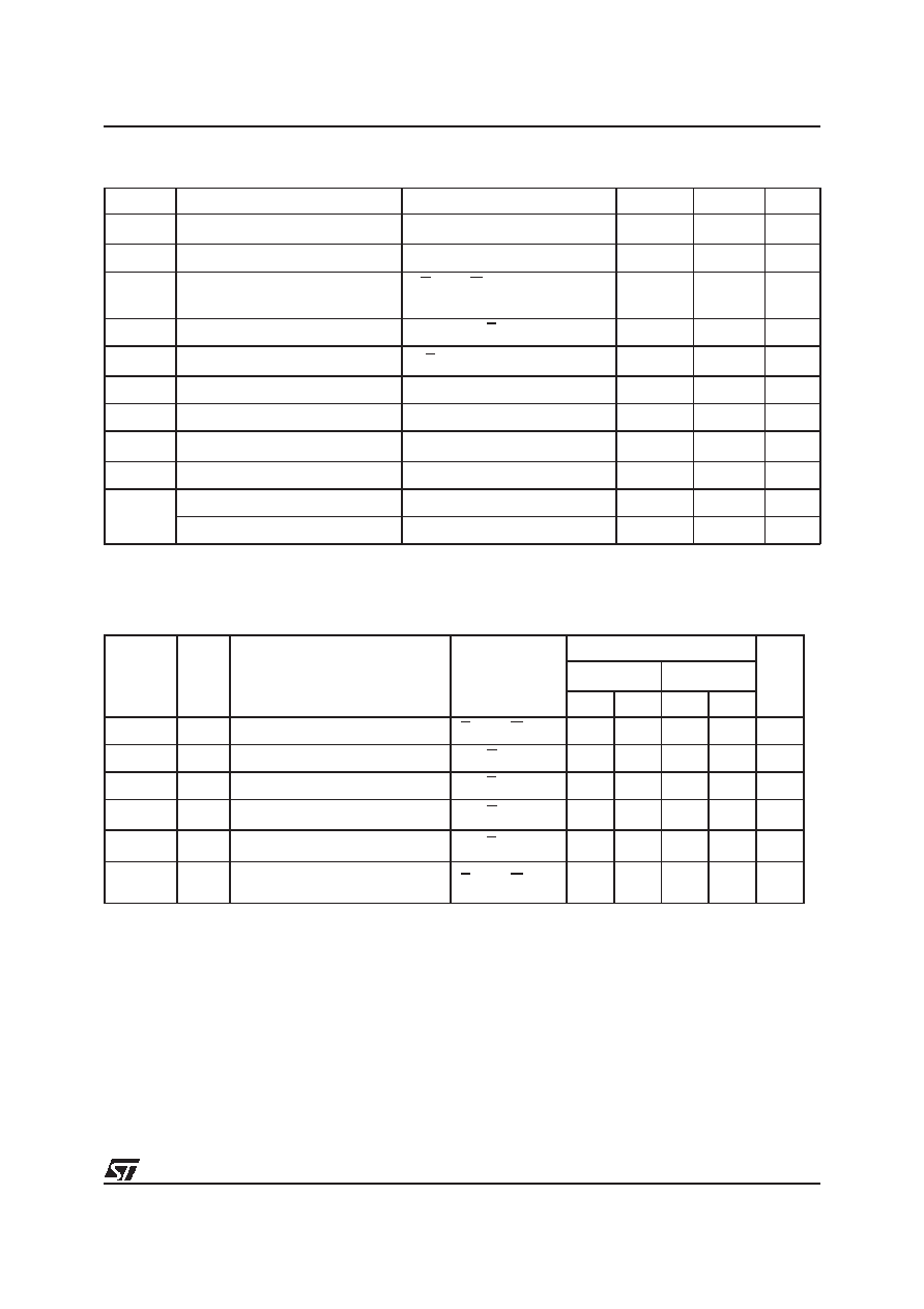
Table 7. Read Mode DC Characteristics (1)
(TA = 0 to 70
°C or –40 to 85°C; VCC = 3.3V ± 10%; VPP =VCC)
Note: 1. VCC must be applied simultaneously with or before VPP and removed simultaneously or after VPP.
2. Maximum DC voltage on Output is VCC +0.5V.
Table 8A. Read Mode AC Characteristics (1)
(TA = 0 to 70 °C or –40 to 85°;VCC = 3.3V ± 10%; VPP =VCC)
Note: 1. VCC must be applied simultaneously with or before VPP and removed simultaneously or after VPP.
2. Sampled only, not 100% tested.
3. Speed obtained with High Speed AC measurement conditions.
Symbol
Parameter
Test Condition
Min
Max
Unit
ILI
Input Leakage Current
0V
≤ VIN ≤ VCC
±10
A
ILO
Output Leakage Current
0V
≤ VOUT ≤ VCC
±10
A
ICC
Supply Current
E=VIL,G= VIL,IOUT = 0mA,
f = 5MHz, VCC ≤ 3.6V
10
mA
ICC1
Supply Current (Standby) TTL
E= VIH
1mA
ICC2
Supply Current (Standby) CMOS
E> VCC –0.2V, VCC ≤ 3.6V
10
A
IPP
Program Current
VPP =VCC
10
A
VIL
Input Low Voltage
–0.3
0.8
V
VIH
(2)
Input High Voltage
2
VCC +1
V
VOL
Output Low Voltage
IOL = 2.1mA
0.4
V
VOH
Output High Voltage TTL
IOH = –400A
2.4
V
Output High Voltage CMOS
IOH = –100A
Vcc – 0.7V
V
Symbol
Alt
Parameter
Test Condition
M27V256
Unit
-90 (3)
-100
Min
Max
Min
Max
tAVQV
tACC
Address Valid to Output Valid
E = VIL,G= VIL
90
100
ns
tELQV
tCE
Chip Enable Low to Output Valid
G= VIL
90
100
ns
tGLQV
tOE
Output Enable Low to Output Valid
E=VIL
40
45
ns
tEHQZ
(2)
tDF
Chip Enable High to Output Hi-Z
G = VIL
025030
ns
tGHQZ
(2)
tDF
Output Enable High to Output Hi-Z
E=VIL
025030
ns
tAXQX
tOH
Address Transition to Output
Transition
E=VIL,G= VIL
00
ns
The associated transient voltage peaks can be
suppressed by complying with the two line output
control and by properly selected decoupling ca-
pacitors. It is recommended that a 0.1
F ceramic
capacitor be used on every device between VCC
and VSS. This should be a high frequency capaci-
tor of low inherent inductance and should be
placed as close to the device as possible. In addi-
tion, a 4.7
F bulk electrolytic capacitor should be
used between VCC and VSS for every eight devic-
es. The bulk capacitor should be located near the
power supply connection point. The purpose of the
bulk capacitor is to overcome the voltage drop
caused by the inductive effects of PCB traces.
相关PDF资料 |
PDF描述 |
|---|---|
| M28840/19AD1P3 | 31 CONTACT(S), ALUMINUM, MALE, CIRCULAR ADAPTER |
| M28840/19AJ1D4 | 155 CONTACT(S), ALUMINUM, MALE, CIRCULAR ADAPTER |
| M28840/19AJ1D5 | 155 CONTACT(S), ALUMINUM, MALE, CIRCULAR ADAPTER |
| M28840/19AJ1D6 | 155 CONTACT(S), ALUMINUM, MALE, CIRCULAR ADAPTER |
| M28840/19AJ1E1 | 155 CONTACT(S), ALUMINUM, FEMALE, CIRCULAR ADAPTER |
相关代理商/技术参数 |
参数描述 |
|---|---|
| M27V256-100F1TR | 制造商:STMICROELECTRONICS 制造商全称:STMicroelectronics 功能描述:256 Kbit 32Kb x 8 Low Voltage UV EPROM and OTP EPROM |
| M27V256-100F6TR | 制造商:STMICROELECTRONICS 制造商全称:STMicroelectronics 功能描述:256 Kbit 32Kb x 8 Low Voltage UV EPROM and OTP EPROM |
| M27V256-100K1TR | 制造商:STMICROELECTRONICS 制造商全称:STMicroelectronics 功能描述:256 Kbit 32Kb x 8 Low Voltage UV EPROM and OTP EPROM |
| M27V256-100K6TR | 制造商:STMICROELECTRONICS 制造商全称:STMicroelectronics 功能描述:256 Kbit 32Kb x 8 Low Voltage UV EPROM and OTP EPROM |
| M27V256-100N1TR | 制造商:STMICROELECTRONICS 制造商全称:STMicroelectronics 功能描述:256 Kbit 32Kb x 8 Low Voltage UV EPROM and OTP EPROM |
发布紧急采购,3分钟左右您将得到回复。