- 您现在的位置:买卖IC网 > PDF目录296348 > M29F016D90M6F (STMICROELECTRONICS) 2M X 8 FLASH 5V PROM, 90 ns, PDSO44 PDF资料下载
参数资料
| 型号: | M29F016D90M6F |
| 厂商: | STMICROELECTRONICS |
| 元件分类: | PROM |
| 英文描述: | 2M X 8 FLASH 5V PROM, 90 ns, PDSO44 |
| 封装: | 0.525 INCH, LEAD FREE, PLASTIC, SOP-44 |
| 文件页数: | 4/37页 |
| 文件大小: | 707K |
| 代理商: | M29F016D90M6F |
第1页第2页第3页当前第4页第5页第6页第7页第8页第9页第10页第11页第12页第13页第14页第15页第16页第17页第18页第19页第20页第21页第22页第23页第24页第25页第26页第27页第28页第29页第30页第31页第32页第33页第34页第35页第36页第37页
Obsolete
Product(s)
- Obsolete
Product(s)
12/37
During Erase Suspend it is possible to Read and
Program cells in blocks that are not being erased;
both Read and Program operations behave as
normal on these blocks. If any attempt is made to
program in a protected block or in the suspended
block then the Program command is ignored and
the data remains unchanged. The Status Register
is not read and no error condition is given. Read-
ing from blocks that are being erased will output
the Status Register.
It is also possible to issue the Auto Select, Read
CFI Query and Unlock Bypass commands during
an Erase Suspend. The Read/Reset command
must be issued to return the device to Read Array
mode before the Resume command will be ac-
cepted.
Erase Resume Command. The Erase Resume
command must be used to restart the Program/
Erase Controller after an Erase Suspend. The de-
vice must be in Read Array mode before the Re-
sume command will be accepted. An erase can be
suspended and resumed more than once.
Read CFI Query Command. The
Read
CFI
Query Command is used to read data from the
Common Flash Interface (CFI) Memory Area. This
command is valid when the device is in the Read
Array mode, or when the device is in Autoselected
mode.
One Bus Write cycle is required to issue the Read
CFI Query Command. Once the command is is-
sued subsequent Bus Read operations read from
the Common Flash Interface Memory Area.
The Read/Reset command must be issued to re-
turn the device to the previous mode (the Read Ar-
ray mode or Autoselected mode). A second Read/
Reset command would be needed if the device is
to be put in the Read Array mode from Autoselect-
ed mode.
for details on the information contained in the
Common Flash Interface (CFI) memory area.
Block Protect and Chip Unprotect Com-
mands. Groups of blocks can be protected
against accidental Program or Erase. The Protec-
The whole chip can be unprotected to allow the
data inside the blocks to be changed.
Block Protect and Chip Unprotect operations are
described in Appendix C.
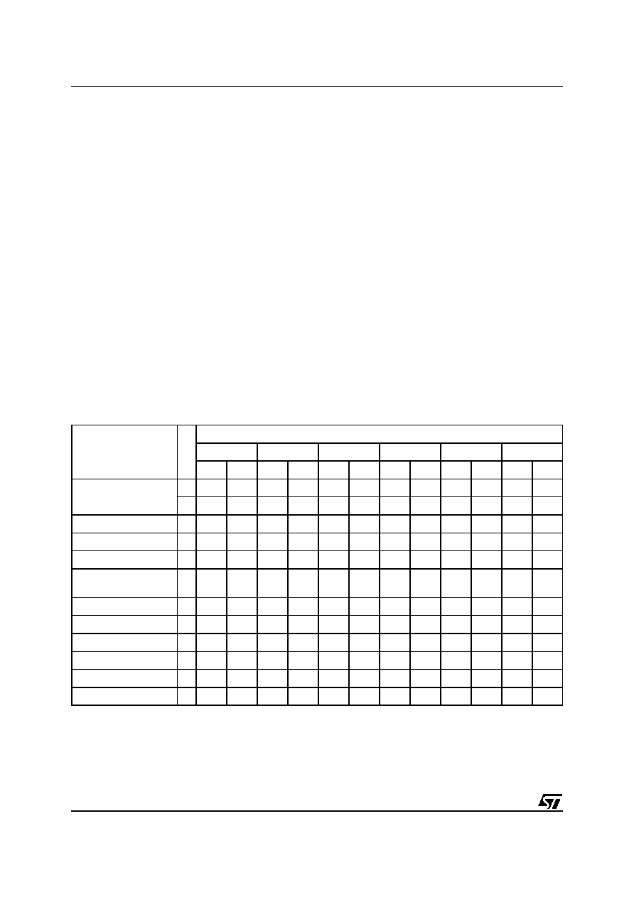
Table 3. Commands
Note: X Don’t Care, PA Program Address, PD Program Data, BA Any address in the Block. All values in the table are in hexadecimal.
Command
Le
ng
th
Bus Write Operations
1st
2nd
3rd
4th
5th
6th
Addr
Data
Addr
Data
Addr
Data
Addr
Data
Addr
Data
Addr
Data
Read/Reset
1X
F0
3555
AA
2AA
55
X
F0
Auto Select
3
555
AA
2AA
55
555
90
Program
4
555
AA
2AA
55
555
A0
PA
PD
Unlock Bypass
3
555
AA
2AA
55
555
20
Unlock Bypass
Program
2
X
A0
PA
PD
Unlock Bypass Reset
2
X
90
X
00
Chip Erase
6
555
AA
2AA
55
555
80
555
AA
2AA
55
555
10
Block Erase
6+
555
AA
2AA
55
555
80
555
AA
2AA
55
BA
30
Erase Suspend
1
X
B0
Erase Resume
1
X
30
Read CFI Query
1
55
98
相关PDF资料 |
PDF描述 |
|---|---|
| M29F016D70N1E | 2M X 8 FLASH 5V PROM, 70 ns, PDSO40 |
| M29F100B-150M3TR | 128K X 8 FLASH 5V PROM, 150 ns, PDSO44 |
| M29F200B-90XM3 | 256K X 8 FLASH 5V PROM, 90 ns, PDSO44 |
| M29F400BB55MT3 | 256K X 16 FLASH 5V PROM, 55 ns, PDSO44 |
| M29F400BB90MT3E | 256K X 16 FLASH 5V PROM, 70 ns, PDSO44 |
相关代理商/技术参数 |
参数描述 |
|---|---|
| M29F016D90M6T | 制造商:STMICROELECTRONICS 制造商全称:STMicroelectronics 功能描述:16 Mbit (2Mb x8, Uniform Block) 5V Supply Flash Memory |
| M29F016D90N1 | 功能描述:闪存 16M (2Mx8) 90ns RoHS:否 制造商:ON Semiconductor 数据总线宽度:1 bit 存储类型:Flash 存储容量:2 MB 结构:256 K x 8 定时类型: 接口类型:SPI 访问时间: 电源电压-最大:3.6 V 电源电压-最小:2.3 V 最大工作电流:15 mA 工作温度:- 40 C to + 85 C 安装风格:SMD/SMT 封装 / 箱体: 封装:Reel |
| M29F016D90N1T | 制造商:STMICROELECTRONICS 制造商全称:STMicroelectronics 功能描述:16 Mbit (2Mb x8, Uniform Block) 5V Supply Flash Memory |
| M29F016D90N6T | 制造商:STMICROELECTRONICS 制造商全称:STMicroelectronics 功能描述:16 Mbit (2Mb x8, Uniform Block) 5V Supply Flash Memory |
| M29F032D | 制造商:STMICROELECTRONICS 制造商全称:STMicroelectronics 功能描述:32 Mbit (4Mb x8, Uniform Block) 5V Supply Flash Memory |
发布紧急采购,3分钟左右您将得到回复。