- 您现在的位置:买卖IC网 > PDF目录80428 > M30624MGP-XXXGP 16-BIT, MROM, 24 MHz, MICROCONTROLLER, PQFP100 PDF资料下载
参数资料
| 型号: | M30624MGP-XXXGP |
| 元件分类: | 微控制器/微处理器 |
| 英文描述: | 16-BIT, MROM, 24 MHz, MICROCONTROLLER, PQFP100 |
| 封装: | 14 X 14 MM, 0.50 MM PITCH, PLASTIC, LQFP-100 |
| 文件页数: | 29/104页 |
| 文件大小: | 1313K |
| 代理商: | M30624MGP-XXXGP |
第1页第2页第3页第4页第5页第6页第7页第8页第9页第10页第11页第12页第13页第14页第15页第16页第17页第18页第19页第20页第21页第22页第23页第24页第25页第26页第27页第28页当前第29页第30页第31页第32页第33页第34页第35页第36页第37页第38页第39页第40页第41页第42页第43页第44页第45页第46页第47页第48页第49页第50页第51页第52页第53页第54页第55页第56页第57页第58页第59页第60页第61页第62页第63页第64页第65页第66页第67页第68页第69页第70页第71页第72页第73页第74页第75页第76页第77页第78页第79页第80页第81页第82页第83页第84页第85页第86页第87页第88页第89页第90页第91页第92页第93页第94页第95页第96页第97页第98页第99页第100页第101页第102页第103页第104页
1. Overview
Page 28 of 96
I : Input
O : Output
I/O : Input and output
NOTES:
1. In this manual, hereafter, VCC refers to VCC1 unless otherwise noted.
2. In M16C/62PT, apply 4.0 to 5.5 V to the VCC1 pin.
3. Ask the oscillator maker the oscillation characteristic.
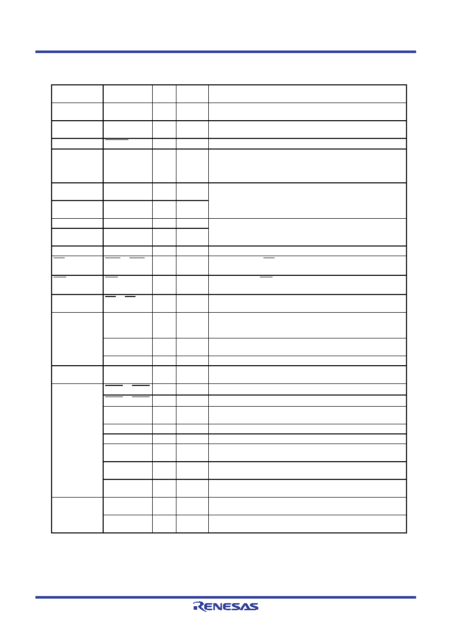
Table 1.20
Pin Description (80-pin Version) (1) (1)
Signal Name
Pin Name
I/O
Type
Power
Supply
Description
Power supply
input
VCC1, VSS
I
Analog power
supply input
AVCC
AVSS
I
VCC1
Applies the power supply for the A/D converter. Connect the
AVCC pin to VCC1. Connect the AVSS pin to VSS.
Reset input
RESET
IVCC1
The microcomputer is in a reset state when applying “L” to the this pin.
CNVSS
(BYTE)
IVCC1
Switches processor mode. Connect this pin to VSS to when after a
reset to start up in single-chip mode. Connect this pin to VCC1 to
start up in microprocessor mode. As for the BYTE pin of the 80-pin
versions, pull-up processing is performed within the microcomputer.
Main clock
input
XIN
I
VCC1
I/O pins for the main clock generation circuit. Connect a ceramic
resonator or crystal oscillator between XIN and XOUT (3). To use
the external clock, input the clock from XIN and leave XOUT
open.
Main clock
output
XOUT
O
VCC1
Sub clock input XCIN
I
VCC1
I/O pins for a sub clock oscillation circuit. Connect a crystal
oscillator between XCIN and XCOUT (3). To use the external
clock, input the clock from XCIN and leave XCOUT open.
Sub clock
output
XCOUT
O
VCC1
Clock output
CLKOUT
O
VCC2
The clock of the same cycle as fC, f8, or f32 is outputted.
INT interrupt
input
INT0 to INT2
I
VCC1
Input pins for the INT interrupt.
NMI interrupt
input
NMI
I
VCC1
Input pin for the NMI interrupt.
Key input
interrupt input
KI0 to KI3
I
VCC1
Input pins for the key input interrupt.
Timer A
TA0OUT,
TA3OUT,
TA4OUT
I/O
VCC1
These are Timer A0,Timer A3 and Timer A4 I/O pins. (however,
output of TA0OUT for the N-channel open drain output.)
TA0IN, TA3IN,
TA4IN
I
VCC1
These are Timer A0, Timer A3 and Timer A4 input pins.
ZP
I
VCC1
Input pin for the Z-phase.
Timer B
TB0IN, TB2IN
to TB5IN
I
VCC1
These are Timer B0, Timer B2 to Timer B5 input pins.
Serial interface CTS0 to CTS1
I
VCC1
These are send control input pins.
RTS0 to RTS1
O
VCC1
These are receive control output pins.
CLK0, CLK1,
CLK3, CLK4
I/O
VCC1
These are transfer clock I/O pins.
RXD0 to RXD2
I
VCC1
These are serial data input pins.
SIN4
I
VCC1
This is serial data input pin.
TXD0 to TXD2
O
VCC1
These are serial data output pins. (however, output of TXD2 for
the N-channel open drain output.)
SOUT3,
SOUT4
O
VCC1
These are serial data output pins.
CLKS1
O
VCC1
This is output pin for transfer clock output from multiple pins
function.
I2C mode
SDA0 to SDA2
I/O
VCC1
These are serial data I/O pins. (however, output of SDA2 for the
N-channel open drain output.)
SCL0 to SCL2
I/O
VCC1
These are transfer clock I/O pins. (however, output of SCL2 for
the N-channel open drain output.)
相关PDF资料 |
PDF描述 |
|---|---|
| M37478E8SP | 8-BIT, OTPROM, 8 MHz, MICROCONTROLLER, PDIP42 |
| MC68HC908GR8AMDW | 8-BIT, FLASH, 8.2 MHz, MICROCONTROLLER, PDSO28 |
| MC9S12DG128CFU | 16-BIT, FLASH, 25 MHz, MICROCONTROLLER, PQFP80 |
| MC9S12DJ128ECFU | 16-BIT, FLASH, 25 MHz, MICROCONTROLLER, PQFP80 |
| MC9S12DJ128EVPV | 16-BIT, FLASH, 25 MHz, MICROCONTROLLER, PQFP112 |
相关代理商/技术参数 |
参数描述 |
|---|---|
| M30624MG-XXXFP | 制造商:RENESAS 制造商全称:Renesas Technology Corp 功能描述:16-BIT SINGLE-CHIP MICROCOMPUTER M16C FAMILY |
| M30624MG-XXXGP | 制造商:RENESAS 制造商全称:Renesas Technology Corp 功能描述:16-BIT SINGLE-CHIP MICROCOMPUTER M16C FAMILY |
| M30624MHP-XXXFP | 制造商:RENESAS 制造商全称:Renesas Technology Corp 功能描述:SINGLE-CHIP 16-BIT CMOS MICROCOMPUTER |
| M30624MHP-XXXGP | 制造商:RENESAS 制造商全称:Renesas Technology Corp 功能描述:SINGLE-CHIP 16-BIT CMOS MICROCOMPUTER |
| M30624MWP | 制造商:RENESAS 制造商全称:Renesas Technology Corp 功能描述:SINGLE-CHIP 16-BIT CMOS MICROCOMPUTER |
发布紧急采购,3分钟左右您将得到回复。