- 您现在的位置:买卖IC网 > PDF目录69010 > M306V7MJA-XXXFP 16-BIT, MROM, 16 MHz, MICROCONTROLLER, PQFP100 PDF资料下载
参数资料
| 型号: | M306V7MJA-XXXFP |
| 元件分类: | 微控制器/微处理器 |
| 英文描述: | 16-BIT, MROM, 16 MHz, MICROCONTROLLER, PQFP100 |
| 封装: | PLASTIC, QFP-100 |
| 文件页数: | 266/298页 |
| 文件大小: | 2272K |
| 代理商: | M306V7MJA-XXXFP |
第1页第2页第3页第4页第5页第6页第7页第8页第9页第10页第11页第12页第13页第14页第15页第16页第17页第18页第19页第20页第21页第22页第23页第24页第25页第26页第27页第28页第29页第30页第31页第32页第33页第34页第35页第36页第37页第38页第39页第40页第41页第42页第43页第44页第45页第46页第47页第48页第49页第50页第51页第52页第53页第54页第55页第56页第57页第58页第59页第60页第61页第62页第63页第64页第65页第66页第67页第68页第69页第70页第71页第72页第73页第74页第75页第76页第77页第78页第79页第80页第81页第82页第83页第84页第85页第86页第87页第88页第89页第90页第91页第92页第93页第94页第95页第96页第97页第98页第99页第100页第101页第102页第103页第104页第105页第106页第107页第108页第109页第110页第111页第112页第113页第114页第115页第116页第117页第118页第119页第120页第121页第122页第123页第124页第125页第126页第127页第128页第129页第130页第131页第132页第133页第134页第135页第136页第137页第138页第139页第140页第141页第142页第143页第144页第145页第146页第147页第148页第149页第150页第151页第152页第153页第154页第155页第156页第157页第158页第159页第160页第161页第162页第163页第164页第165页第166页第167页第168页第169页第170页第171页第172页第173页第174页第175页第176页第177页第178页第179页第180页第181页第182页第183页第184页第185页第186页第187页第188页第189页第190页第191页第192页第193页第194页第195页第196页第197页第198页第199页第200页第201页第202页第203页第204页第205页第206页第207页第208页第209页第210页第211页第212页第213页第214页第215页第216页第217页第218页第219页第220页第221页第222页第223页第224页第225页第226页第227页第228页第229页第230页第231页第232页第233页第234页第235页第236页第237页第238页第239页第240页第241页第242页第243页第244页第245页第246页第247页第248页第249页第250页第251页第252页第253页第254页第255页第256页第257页第258页第259页第260页第261页第262页第263页第264页第265页当前第266页第267页第268页第269页第270页第271页第272页第273页第274页第275页第276页第277页第278页第279页第280页第281页第282页第283页第284页第285页第286页第287页第288页第289页第290页第291页第292页第293页第294页第295页第296页第297页第298页
Rev.1.00
May 18, 2004
page 7 of 296
M306V7MG/MH/MJ/MJA-XXXFP, M306V7FG/FH/FJ/FJAFP
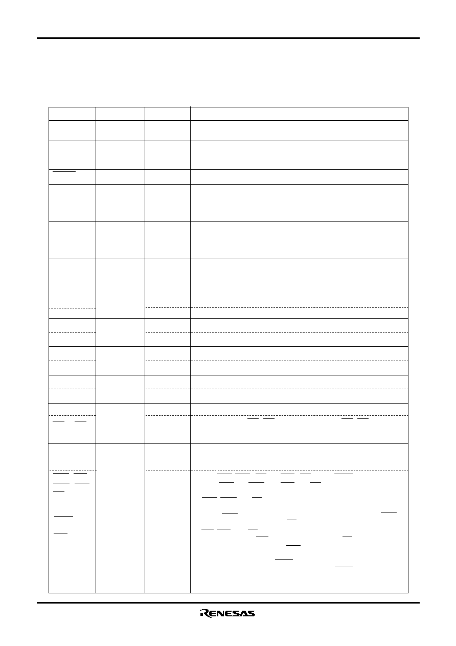
Table 1.5.3 Pin description (1)
VCCE, VCCI,
VSS
CNVSS
XIN
XOUT
BYTE
P00 to P07
Signal name
Power supply
input
CNVSS
Reset input
Clock input
Clock output
External data
bus width
select input
I/O port P0
Supply 4.75V to 5.25V to the VCCE pin. Supply 3.15V to 3.45V to the
VCCI pin. Supply 0V to the VSS pin.
Function
This pin switches between processor modes. Connect it to the
VSS pin when operating in single-chip or memory expansion mode.
Connect it to the VCCI pin when in microprocessor mode.
A “L” on this input resets the microcomputer.
These pins are provided for the main clock generating circuit.Connect
a ceramic resonator or crystal between the XIN and the XOUT pins. To
use an externally derived clock, input it to the XIN pin and leave the
XOUT pin open.
This pin selects the width of an external data bus. A 16-bit width is
selected when this input is “L”; an 8-bit width is selected when this
input is “H”. This input must be fixed to either “H” or “L.” When
operating in single-chip mode,connect this pin to VSS.
This is an 8-bit CMOS I/O port. It has an input/output port direction
register that allows the user to set each pin for input or output
individually. When set for input in single-chip mode, the user can specify
in units of four bits via software whether or not they are tied to a pull-up
resistor. In memory expansion and microprocessor modes, the user
cannot specify that.
Pin name
Input
Output
Input
Input/output
I/O type
D0 to D7
P10 to P17
I/O port P1
07
These pins input and output data (D –D ).
This is an 8-bit I/O port equivalent to P0.
Input/output
D8 to D15
P20 to P27
A0 to A7
P30 to P37
A8 to A15
P40 to P47
I/O port P2
I/O port P3
I/O port P4
These pins input and output data (D8–D15).
This is an 8-bit I/O port equivalent to P0.
These pins output 8 low-order address bits (A0–A7).
This is an 8-bit I/O port equivalent to P0.
These pins output 8 middle-order address bits (A8–A15).
This is an 8-bit I/O port equivalent to P0.
Input/output
Output
Input/output
Output
Input/output
Output
CS0 to CS3,
A16 to A19
These pins output CS0–CS3 signals and A16–A19. CS0–CS3 are chip
select signals used to specify an access space. A16–A19 are 4 high-
order address bits.
RESET
I/O port P5
P50 to P57
This is an 8-bit I/O port equivalent to P0. In single-chip mode, P57 in
this port outputs a divide-by-8 or divide-by-32 clock of XIN or a clock of
the same frequency as XCIN as selected by software.
Output
Input
Output
Input
WRL / WR,
WRH / BHE,
RD,
BCLK,
HLDA,
HOLD,
ALE,
RDY
Output WRL, WRH (WR and BHE), RD, BCLK, HLDA, and ALE
signals. WRL and WRH, and BHE and WR can be switched using
software control.
s WRL, WRH, and RD selected
With a 16-bit external data bus, data is written to even addresses
when the WRL signal is “L” and to the odd addresses when the WRH
signal is “L”. Data is read when RD is “L”.
s WR, BHE, and RD selected
Data is written when WR is “L”. Data is read when RD is “L”. Odd
addresses are accessed when BHE is “L”. Use this mode when using
an 8-bit external data bus.
While the input level at the HOLD pin is “L”, the microcomputer is
placed in the hold state. While in the hold state, HLDA outputs a “L”
level. While the input level of the RDY pin is “L”, the microcomputer is in
the ready state. ALE output is indefinite.
Input/output
相关PDF资料 |
PDF描述 |
|---|---|
| M30833FJFP | 32-BIT, FLASH, 30 MHz, MICROCONTROLLER, PQFP100 |
| M30833MJFP | 32-BIT, MROM, 30 MHz, MICROCONTROLLER, PQFP100 |
| M30833MJGP | 32-BIT, MROM, 30 MHz, MICROCONTROLLER, PQFP100 |
| M30835MJGP | 32-BIT, MROM, 30 MHz, MICROCONTROLLER, PQFP144 |
| M30865FJGP | 32-BIT, FLASH, 32 MHz, MICROCONTROLLER, PQFP144 |
相关代理商/技术参数 |
参数描述 |
|---|---|
| M306V7MJ-XXXFP | 制造商:RENESAS 制造商全称:Renesas Technology Corp 功能描述:SINGLE-CHIP 16-BIT CMOS MICROCOMPUTER with CLOSED CAPTION DECODER and ON-SCREEN DISPLAY CONTROLLER |
| M306V7T-RPD-E | 功能描述:DEV EMULATION POD FOR M16C/6V (M RoHS:否 类别:编程器,开发系统 >> 配件 系列:- 产品培训模块:Lead (SnPb) Finish for COTS Obsolescence Mitigation Program RoHS指令信息:IButton RoHS Compliance Plan 标准包装:1 系列:- 附件类型:USB 至 1-Wire? RJ11 适配器 适用于相关产品:1-Wire? 设备 产品目录页面:1429 (CN2011-ZH PDF) |
| M306V8FJFP | 制造商:RENESAS 制造商全称:Renesas Technology Corp 功能描述:SINGLE-CHIP 16-BIT CMOS MICROCOMPUTER |
| M3-076 | 制造商:Southco 功能描述: |
| M3077 | 制造商:Tamura Corporation of America 功能描述: |
发布紧急采购,3分钟左右您将得到回复。