- 您现在的位置:买卖IC网 > PDF目录69010 > M306V7MJA-XXXFP 16-BIT, MROM, 16 MHz, MICROCONTROLLER, PQFP100 PDF资料下载
参数资料
| 型号: | M306V7MJA-XXXFP |
| 元件分类: | 微控制器/微处理器 |
| 英文描述: | 16-BIT, MROM, 16 MHz, MICROCONTROLLER, PQFP100 |
| 封装: | PLASTIC, QFP-100 |
| 文件页数: | 75/298页 |
| 文件大小: | 2272K |
| 代理商: | M306V7MJA-XXXFP |
第1页第2页第3页第4页第5页第6页第7页第8页第9页第10页第11页第12页第13页第14页第15页第16页第17页第18页第19页第20页第21页第22页第23页第24页第25页第26页第27页第28页第29页第30页第31页第32页第33页第34页第35页第36页第37页第38页第39页第40页第41页第42页第43页第44页第45页第46页第47页第48页第49页第50页第51页第52页第53页第54页第55页第56页第57页第58页第59页第60页第61页第62页第63页第64页第65页第66页第67页第68页第69页第70页第71页第72页第73页第74页当前第75页第76页第77页第78页第79页第80页第81页第82页第83页第84页第85页第86页第87页第88页第89页第90页第91页第92页第93页第94页第95页第96页第97页第98页第99页第100页第101页第102页第103页第104页第105页第106页第107页第108页第109页第110页第111页第112页第113页第114页第115页第116页第117页第118页第119页第120页第121页第122页第123页第124页第125页第126页第127页第128页第129页第130页第131页第132页第133页第134页第135页第136页第137页第138页第139页第140页第141页第142页第143页第144页第145页第146页第147页第148页第149页第150页第151页第152页第153页第154页第155页第156页第157页第158页第159页第160页第161页第162页第163页第164页第165页第166页第167页第168页第169页第170页第171页第172页第173页第174页第175页第176页第177页第178页第179页第180页第181页第182页第183页第184页第185页第186页第187页第188页第189页第190页第191页第192页第193页第194页第195页第196页第197页第198页第199页第200页第201页第202页第203页第204页第205页第206页第207页第208页第209页第210页第211页第212页第213页第214页第215页第216页第217页第218页第219页第220页第221页第222页第223页第224页第225页第226页第227页第228页第229页第230页第231页第232页第233页第234页第235页第236页第237页第238页第239页第240页第241页第242页第243页第244页第245页第246页第247页第248页第249页第250页第251页第252页第253页第254页第255页第256页第257页第258页第259页第260页第261页第262页第263页第264页第265页第266页第267页第268页第269页第270页第271页第272页第273页第274页第275页第276页第277页第278页第279页第280页第281页第282页第283页第284页第285页第286页第287页第288页第289页第290页第291页第292页第293页第294页第295页第296页第297页第298页
Rev.1.00
May 18, 2004
page 166 of 296
M306V7MG/MH/MJ/MJA-XXXFP, M306V7FG/FH/FJ/FJAFP
2.14.2 Clamping Circuit and Low-pass Filter
The clamp circuit clamps the sync. tip part of the composite video signal input from the CVIN pin. The low-
pass filter attenuates the noise of clamped composite video signal. The CVIN pin to which composite video
signal is input requires a capacitor (0.1
F) coupling outside. Pull down the CVIN pin with a resistor of
hundreds of kiloohms to 1 M
. In addition, we recommend to install externally a simple low-pass filter
using a resistor and a capacitor at the CVIN pin (refer to Figure 2.14.1 and notes).
2.14.3 Sync Slice Circuit
This circuit takes out a composite sync signal from the output signal of the low-pass filter.
Set bit 6 and 7 to 11b of ID1 reserved register (addresses 037C16 and 031D16) show in Fig 2.14.21.
2.14.4 Synchronous Signal Separation Circuit
This circuit separates a horizontal synchronous signal and a vertical synchronous signal from the compos-
ite sync signal taken out in the sync slice circuit.
(1) Horizontal synchronous signal (Hsep)
A one-shot horizontal synchronizing signal Hsep is generated at the falling edge of the composite sync
signal.
(2) Vertical synchronous signal (Vsep)
As a Vsep signal generating method, it is possible to select one of the following 2 methods by using bit
4 of the data slicer control register 2 (address 026116/030116).
Method 1 The “L” level width of the composite sync signal is measured. If this width exceeds a
certain time, a Vsep signal is generated in synchronization with the rising of the timing
signal immediately after this “L” level.
Method 2 The “L” level width of the composite sync signal is measured. If this width exceeds a
certain time, it is detected whether a falling of the composite sync signal exits or not in the
“L” level period of the timing signal immediately after this “L” level. If a falling exists, a Vsep
signal is generated in synchronization with the rising of the timing signal (refer to Figure
2.14.6).
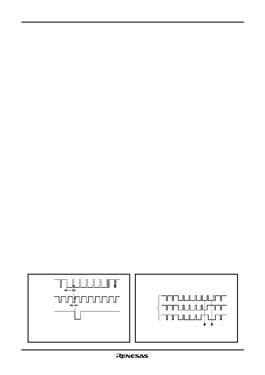
Figure 2.14.6 shows a Vsep generating timing. The timing signal shown in the figure is generated from the
reference clock which the timing generating circuit outputs.
Reading bit 5 of data slicer control register 2 permits determinating the shape of the V-pulse portion of the
composite sync signal. As shown in Figure 2.14.7, when the A level matches the B level, this bit is “0.” In
the case of a mismatch, the bit is “1.”
Figure 2.14.6 Vsep generating timing (method 2)
Composite sync
“L” level width is measured
“L” level period of a timing signal
Timing
signal
A Vsep signal is generated at a rising of the timing signal
immediately after the “L” level width of the composite
sync signal exceeds a certain time.
Vsep signal
Figure 2.14.7 Determination of v-pulse waveform
Composite
sync signal
A
B
0
1
Bit 5 of
DSC02/DSC12
相关PDF资料 |
PDF描述 |
|---|---|
| M30833FJFP | 32-BIT, FLASH, 30 MHz, MICROCONTROLLER, PQFP100 |
| M30833MJFP | 32-BIT, MROM, 30 MHz, MICROCONTROLLER, PQFP100 |
| M30833MJGP | 32-BIT, MROM, 30 MHz, MICROCONTROLLER, PQFP100 |
| M30835MJGP | 32-BIT, MROM, 30 MHz, MICROCONTROLLER, PQFP144 |
| M30865FJGP | 32-BIT, FLASH, 32 MHz, MICROCONTROLLER, PQFP144 |
相关代理商/技术参数 |
参数描述 |
|---|---|
| M306V7MJ-XXXFP | 制造商:RENESAS 制造商全称:Renesas Technology Corp 功能描述:SINGLE-CHIP 16-BIT CMOS MICROCOMPUTER with CLOSED CAPTION DECODER and ON-SCREEN DISPLAY CONTROLLER |
| M306V7T-RPD-E | 功能描述:DEV EMULATION POD FOR M16C/6V (M RoHS:否 类别:编程器,开发系统 >> 配件 系列:- 产品培训模块:Lead (SnPb) Finish for COTS Obsolescence Mitigation Program RoHS指令信息:IButton RoHS Compliance Plan 标准包装:1 系列:- 附件类型:USB 至 1-Wire? RJ11 适配器 适用于相关产品:1-Wire? 设备 产品目录页面:1429 (CN2011-ZH PDF) |
| M306V8FJFP | 制造商:RENESAS 制造商全称:Renesas Technology Corp 功能描述:SINGLE-CHIP 16-BIT CMOS MICROCOMPUTER |
| M3-076 | 制造商:Southco 功能描述: |
| M3077 | 制造商:Tamura Corporation of America 功能描述: |
发布紧急采购,3分钟左右您将得到回复。