- 您现在的位置:买卖IC网 > PDF目录69012 > M35500BGP FLUORESCENT DSPL CTRL, PQFP44 PDF资料下载
参数资料
| 型号: | M35500BGP |
| 元件分类: | 显示控制器 |
| 英文描述: | FLUORESCENT DSPL CTRL, PQFP44 |
| 封装: | 10 X 10 MM, 0.80 MM PITCH, PLASTIC, QFP-44 |
| 文件页数: | 1/16页 |
| 文件大小: | 169K |
| 代理商: | M35500BGP |
1
MITSUBISHI <DIGITAL ASSP>
M35500AFP/BGP
FLD(VFD) CONTROLLER
DESCRIPTION/FEATURES
High-breakdown-voltage output port ......................................... 26
Segment output ............................................ 8 to 18
Digit output ................................................... 7 to 10
(Ports P0 to P7 are also used as ordinary output ports)
Output breakdown .................................. Vcc – 45 V
Output current .................. –18 mA (DIG0 to DIG17),
–7 mA (SEG0 to SEG7)
Pull-down resistor ........................................ build-in
Dimmer switch ............................................ 4 levels
A-D converter ................................................... 8-bit ! 6 channels
Absolute accuracy ....................................... ±3 LSB
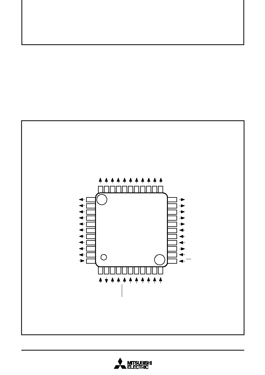
PIN CONFIGURATION (TOP VIEW)
Serial I/O ..................................... 4 (CS controller, external clock)
Noise filter .................................................... build-in
(in serial input pin and clock pin, 2 MHz sampling)
FLD display data ............................................. input
A-D conversion data ..................................... output
Command ....................................................... input
Package ................................................................. 44P6N/44P6X
Oscillating circuit ........... RC oscillating cirucit (external capacitor)
Oscillating frequency ..................................... 4 MHz
Power source voltage .................................................. 4.0 to 5.5 V
Fig. 1. Pin configuration of M35500AFP/BGP
Package type: 44P6N-A/44P6X
1
22
M35500AFP
M35500BGP
3
2
3
0
3
1
2
9
2
6
2
8
2
7
2
5
2
4
2
3
D
IG
1
5
/S
E
G
1
0
D
IG
1
4
/S
E
G
1
D
IG
1
3
/S
E
G
1
2
D
IG
1
2
/S
E
G
1
3
D
IG
1
/S
E
G
1
4
D
IG
1
0
/S
E
G
1
5
D
IG
9
/S
E
G
1
6
D
IG
8
/S
E
G
1
7
D
IG
6
/P
6
D
IG
7
/P
7
D
IG
5
/P
5
DIG16/SEG9
DIG17/SEG8
SEG7
SEG6
SEG5
SEG4
SEG3
SEG2
SEG1
SEG0
VDD
34
35
36
37
38
39
40
41
42
43
44
V
D
X
O
U
T
V
S
X
IN
R
E
S
E
T
A
N
5
A
N
4
A
N
3
A
N
2
A
N
1
A
N
0
DIG4/P4
DIG3/P3
DIG2/P2
DIG1/P1
DIG0/P0
VEE
SCLK
SOUT
SIN
CS
2
3
4
5
6
7
8
9
1
0
1
21
20
19
18
17
16
15
14
13
12
相关PDF资料 |
PDF描述 |
|---|---|
| M35500AFP | FLUORESCENT DSPL CTRL, PQFP44 |
| M37150M8-XXXFP | 8-BIT, MROM, 8.95 MHz, MICROCONTROLLER, PDSO42 |
| M37150MF-XXXFP | 8-BIT, MROM, 8.95 MHz, MICROCONTROLLER, PDSO42 |
| M37150EFFP | 8-BIT, OTPROM, 8.95 MHz, MICROCONTROLLER, PDSO42 |
| M37151M6-XXXFP | 8-BIT, MROM, 8.1 MHz, MICROCONTROLLER, PDSO42 |
相关代理商/技术参数 |
参数描述 |
|---|---|
| M35501FP | 制造商:MITSUBISHI 制造商全称:Mitsubishi Electric Semiconductor 功能描述:FLD(VFD) DIGIT EXPANDER |
| M35502AFP | 制造商:MITSUBISHI 制造商全称:Mitsubishi Electric Semiconductor 功能描述:FLD CONTROLLER |
| M3554 | 制造商:Baldor Electric Company 功能描述: |
| M3558 | 制造商:BALDOR MOTORS 功能描述: 制造商:Baldor Electric Company 功能描述: |
| M3558T | 制造商:BALDOR MOTORS 功能描述: |
发布紧急采购,3分钟左右您将得到回复。