- 您现在的位置:买卖IC网 > PDF目录383294 > M366S3253BTS (SAMSUNG SEMICONDUCTOR CO. LTD.) 32Mx64 SDRAM DIMM based on 32Mx8, 4Banks, 8K Refresh, 3.3V Synchronous DRAMs with SPD PDF资料下载
参数资料
| 型号: | M366S3253BTS |
| 厂商: | SAMSUNG SEMICONDUCTOR CO. LTD. |
| 英文描述: | 32Mx64 SDRAM DIMM based on 32Mx8, 4Banks, 8K Refresh, 3.3V Synchronous DRAMs with SPD |
| 中文描述: | 32Mx64 SDRAM的内存在32Mx8,4Banks,8K的刷新,3.3社民党基于同步DRAM |
| 文件页数: | 9/10页 |
| 文件大小: | 115K |
| 代理商: | M366S3253BTS |
PC133 Unbuffered DIMM
M366S3253BTS
REV. 0.1 July. 2000
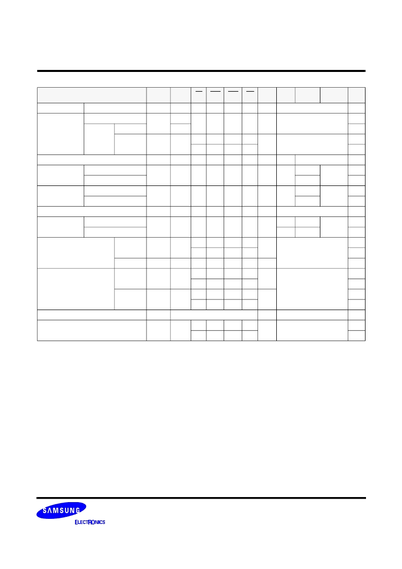
SIMPLIFIED TRUTH TABLE
(V=Valid, X=Don
′
t care, H=Logic high, L=Logic low)
1. OP Code : Operand code
A
0
~ A
12
& BA
0
~ BA
1
: Program keys. (@ MRS)
2. MRS can be issued only at all banks precharge state.
A new command can be issued after 2 clock cycles of MRS.
3. Auto refresh functions are as same as CBR refresh of DRAM.
The automatical precharge without row precharge command is meant by "Auto".
Auto/self refresh can be issued only at all banks precharge state.
4. BA
0
~ BA
1
: Bank select addresses.
If both BA
0
and BA
1
are "Low" at read, write, row active and precharge, bank A is selected.
If both BA
0
is "High" and BA
1
is "Low" at read, write, row active and precharge, bank B is selected.
If both BA
0
is "Low" and BA
1
is "High" at read, write, row active and precharge, bank C is selected.
If both BA
0
and BA
1
are "High" at read, write, row active and precharge, bank D is selected.
If A
10
/AP is "High" at row precharge, BA
0
and BA
1
is ignored and all banks are selected.
5. During burst read or write with auto precharge, new read/write command can not be issued.
Another bank read/write command can be issued after the end of burst.
New row active of the associated bank can be issued at t
RP
after the end of burst.
6. Burst stop command is valid at every burst length.
7. DQM sampled at positive going edge of a CLK and masks the data-in at the very CLK (Write DQM latency is 0),
but makes Hi-Z state the data-out of 2 CLK cycles after. (Read DQM latency is 2)
Command
CKEn-1
CKEn
CS
RAS
CAS
WE
DQM
BA
0,1
A
10
/AP
A
12
, A
11,
A
9
~ A
0
Note
Register
Mode register set
H
X
L
L
L
L
X
OP code
1,2
Refresh
Auto refresh
H
H
L
L
L
H
X
X
3
Self
refresh
Entry
L
3
Exit
L
H
L
H
H
H
X
X
3
H
X
X
X
3
Bank active & row addr.
H
X
L
L
H
H
X
V
Row address
Read &
column address
Auto precharge disable
H
X
L
H
L
H
X
V
L
Column
address
(A
0
~ A
9
)
4
Auto precharge enable
H
4,5
Write &
column address
Auto precharge disable
H
X
L
H
L
L
X
V
L
Column
address
(A
0
~ A
9
)
4
Auto precharge enable
H
4,5
Burst stop
H
X
L
H
H
L
X
X
6
Precharge
Bank selection
H
X
L
L
H
L
X
V
L
X
All banks
X
H
Clock suspend or
active power down
Entry
H
L
H
X
X
X
X
X
L
V
V
V
Exit
L
H
X
X
X
X
X
Precharge power down mode
Entry
H
L
H
X
X
X
X
X
L
H
H
H
Exit
L
H
H
X
X
X
X
L
V
V
V
DQM
H
V
X
7
No operation command
H
X
H
X
X
X
X
X
L
H
H
H
Notes :
X
相关PDF资料 |
PDF描述 |
|---|---|
| M366S3253BTS-C75 | 32Mx64 SDRAM DIMM based on 32Mx8, 4Banks, 8K Refresh, 3.3V Synchronous DRAMs with SPD |
| M366S3323DTS | 32Mx64 SDRAM DIMM based on 16Mx8, 4Banks, 4K Refresh, 3.3V Synchronous DRAMs with SPD |
| M366S3323DTS-C1H | 32Mx64 SDRAM DIMM based on 16Mx8, 4Banks, 4K Refresh, 3.3V Synchronous DRAMs with SPD |
| M366S3323DTS-C1L | 32Mx64 SDRAM DIMM based on 16Mx8, 4Banks, 4K Refresh, 3.3V Synchronous DRAMs with SPD |
| M366S3323DTS-C7A | 32Mx64 SDRAM DIMM based on 16Mx8, 4Banks, 4K Refresh, 3.3V Synchronous DRAMs with SPD |
相关代理商/技术参数 |
参数描述 |
|---|---|
| M366S3253BTS-C75 | 制造商:SAMSUNG 制造商全称:Samsung semiconductor 功能描述:32Mx64 SDRAM DIMM based on 32Mx8, 4Banks, 8K Refresh, 3.3V Synchronous DRAMs with SPD |
| M366S3253CTS | 制造商:SAMSUNG 制造商全称:Samsung semiconductor 功能描述:32Mx64 SDRAM DIMM based on 32Mx8, 4Banks, 8K Refresh, 3.3V Synchronous DRAMs with SPD |
| M366S3253CTS-C1H | 制造商:SAMSUNG 制造商全称:Samsung semiconductor 功能描述:32Mx64 SDRAM DIMM based on 32Mx8, 4Banks, 8K Refresh, 3.3V Synchronous DRAMs with SPD |
| M366S3253CTS-C1L | 制造商:SAMSUNG 制造商全称:Samsung semiconductor 功能描述:32Mx64 SDRAM DIMM based on 32Mx8, 4Banks, 8K Refresh, 3.3V Synchronous DRAMs with SPD |
| M366S3253CTS-C7A | 制造商:SAMSUNG 制造商全称:Samsung semiconductor 功能描述:32Mx64 SDRAM DIMM based on 32Mx8, 4Banks, 8K Refresh, 3.3V Synchronous DRAMs with SPD |
发布紧急采购,3分钟左右您将得到回复。