- 您现在的位置:买卖IC网 > PDF目录224142 > M38030F8L-XXXHP (Renesas Technology Corp.) SINGLE-CHIP 8-BIT CMOS MICROCOMPUTER PDF资料下载
参数资料
| 型号: | M38030F8L-XXXHP |
| 厂商: | Renesas Technology Corp. |
| 英文描述: | SINGLE-CHIP 8-BIT CMOS MICROCOMPUTER |
| 中文描述: | 单芯片8位CMOS微机 |
| 文件页数: | 86/119页 |
| 文件大小: | 1575K |
| 代理商: | M38030F8L-XXXHP |
第1页第2页第3页第4页第5页第6页第7页第8页第9页第10页第11页第12页第13页第14页第15页第16页第17页第18页第19页第20页第21页第22页第23页第24页第25页第26页第27页第28页第29页第30页第31页第32页第33页第34页第35页第36页第37页第38页第39页第40页第41页第42页第43页第44页第45页第46页第47页第48页第49页第50页第51页第52页第53页第54页第55页第56页第57页第58页第59页第60页第61页第62页第63页第64页第65页第66页第67页第68页第69页第70页第71页第72页第73页第74页第75页第76页第77页第78页第79页第80页第81页第82页第83页第84页第85页当前第86页第87页第88页第89页第90页第91页第92页第93页第94页第95页第96页第97页第98页第99页第100页第101页第102页第103页第104页第105页第106页第107页第108页第109页第110页第111页第112页第113页第114页第115页第116页第117页第118页第119页
Rev.1.00
Apr 2, 2007
Page 69 of 117
REJ03B0212-0100
3803 Group (Spec.L)
FLASH MEMORY MODE
The 3803 group (Spec.L)’s flash memory version has the flash
memory that can be rewritten with a single power source.
For this flash memory, three flash memory modes are available
in which to read, program, and erase: the parallel I/O and
standard serial I/O modes in which the flash memory can be
manipulated using a programmer and the CPU rewrite mode in
which the flash memory can be manipulated by the Central
Processing Unit (CPU).
This flash memory version has some blocks on the flash memory
as shown in Figure 67 and each block can be erased.
In addition to the ordinary User ROM area to store the MCU
operation control program, the flash memory has a Boot ROM
area that is used to store a program to control rewriting in CPU
rewrite and standard serial I/O modes. This Boot ROM area has
had a standard serial I/O mode control program stored in it when
shipped from the factory. However, the user can write a rewrite
control program in this area that suits the user’s application
system. This Boot ROM area can be rewritten in only parallel I/O
mode.
Summary
Table 9 lists the summary of the 3803 group (Spec.L) flash
memory version.
NOTE:
1. The Boot ROM area has had a standard serial I/O mode control program stored in it when shipped from the factory.
This Boot ROM area can be erased and written in only parallel I/O mode.
NOTES:
1. VCC = AVCC = 2.7 V to 5.5 V, Topr = 0
°C to 60 °C, unless otherwise noted.
2. Definition of programming/erase count
The programming/erase count refers to the number of erase operations per block. For example, if block A is a 2 Kbyte block and
2,048 1-byte writes are performed, all to different addresses, after which block A is erased, the programming/erase count is 1. Note
that for each erase operation it is not possible to perform more than one programming (write) operation to the same address
(overwrites prohibited).
3. This is the number of times for which all electrical characteristics are guaranteed after a programming or erase operation. (The
guarantee covers the range from 1 to maximum value.)
4. On systems where reprogramming is performed a large number of times, it is possible to reduce the effective number of overwrites
by sequentially shifting the write address, so that as much of the available area of the block is used up through successive
programming (write) operations before an erase operation is performed. For example, if each programming operation uses 16 bytes
of space, a maximum of 128 programming operations may be performed before it becomes necessary to erase the block in order to
continue. In this way the effective number of overwrites can be kept low. The effective overwrite count can be further reduced by
evenly dividing operations between block A and block B. It is recommended that data be retained on the number of times each
block has been erased and a limit count set.
5. If a block erase error occurs, execute the clear status register command followed by the block erase command a minimum of three
times and until the erase error is no longer generated.
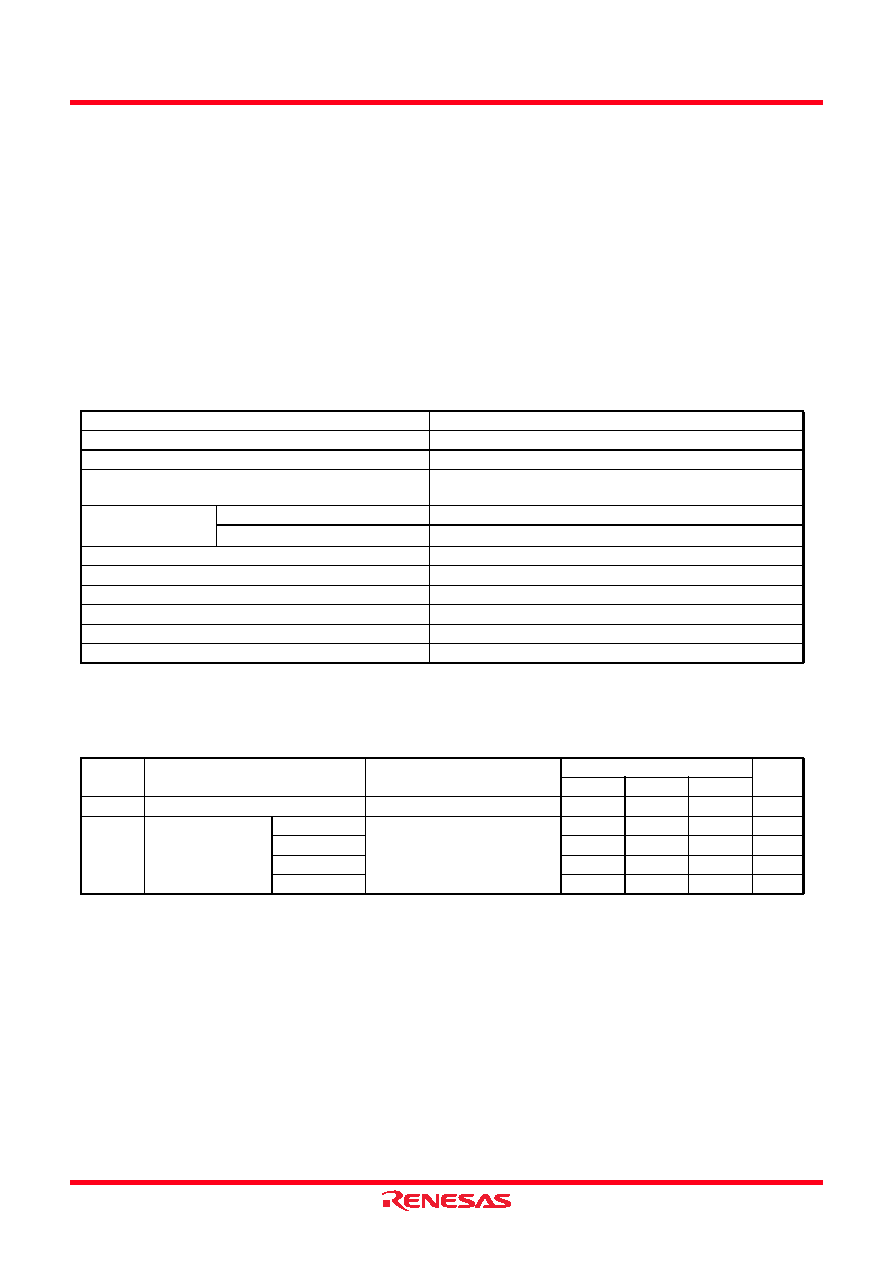
Table 9
Summary of 3803 group (Spec.L)’s flash memory version
Item
Specifications
Power source voltage (VCC)VCC = 2.7 to 5.5 V
Program/Erase VPP voltage (VPP)VCC = 2.7 to 5.5 V
Flash memory mode
3 modes; Parallel I/O mode, Standard serial I/O mode, CPU
rewrite mode
Erase block division
User ROM area/Data ROM area
Refer to Figure 67.
Boot ROM area (1)
Not divided (4 Kbytes)
Program method
In units of bytes
Erase method
Block erase
Program/Erase control method
Program/Erase control by software command
Number of commands
5 commands
Number of program/Erase times
100(Max.)
ROM code protection
Available in parallel I/O mode and standard serial I/O mode
Table 10 Electrical characteristics of flash memory (program ROM)
Symbol
Parameter
Test conditions
Limits
Unit
Min.
Typ.
Max.
Byte programming time
VCC = 5.0 V, Topr = 25
°C
60
400
s
Block erase time
(Block 1)
VCC = 5.0 V, Topr = 25
°C
0.5
9
s
(Block 2)
0.9
9
s
(Block 3)
1.3
9
s
(Block A, B)
0.3
9
s
相关PDF资料 |
PDF描述 |
|---|---|
| M38030F8L-XXXKP | SINGLE-CHIP 8-BIT CMOS MICROCOMPUTER |
| M38030F8L-XXXSP | SINGLE-CHIP 8-BIT CMOS MICROCOMPUTER |
| M38030F8L-XXXWG | SINGLE-CHIP 8-BIT CMOS MICROCOMPUTER |
| M381-L-109-5121LF | 9 CONTACT(S), MALE, STRAIGHT TWO PART BOARD CONNECTOR, SOLDER |
| M381-L-109-5221LF | 9 CONTACT(S), MALE, STRAIGHT TWO PART BOARD CONNECTOR, SOLDER |
相关代理商/技术参数 |
参数描述 |
|---|---|
| M38037M5H-175HP#U0 | 制造商:Renesas Electronics Corporation 功能描述:8BIT CISC - Trays |
| M38037M8108F | 制造商:Panasonic Industrial Company 功能描述:IC |
| M38037M8H-194HP#U0 | 制造商:Renesas Electronics Corporation 功能描述:8BIT CISC - Trays |
| M38039FFHFP#U0 | 功能描述:IC 740 MCU FLASH 60K 64QFP RoHS:是 类别:集成电路 (IC) >> 嵌入式 - 微控制器, 系列:740/38000 产品培训模块:CAN Basics Part-1 CAN Basics Part-2 Electromagnetic Noise Reduction Techniques Part 1 M16C Product Overview Part 1 M16C Product Overview Part 2 标准包装:1 系列:M16C™ M32C/80/87 核心处理器:M32C/80 芯体尺寸:16/32-位 速度:32MHz 连通性:EBI/EMI,I²C,IEBus,IrDA,SIO,UART/USART 外围设备:DMA,POR,PWM,WDT 输入/输出数:121 程序存储器容量:384KB(384K x 8) 程序存储器类型:闪存 EEPROM 大小:- RAM 容量:24K x 8 电压 - 电源 (Vcc/Vdd):3 V ~ 5.5 V 数据转换器:A/D 34x10b,D/A 2x8b 振荡器型:内部 工作温度:-20°C ~ 85°C 封装/外壳:144-LQFP 包装:托盘 产品目录页面:749 (CN2011-ZH PDF) 配用:R0K330879S001BE-ND - KIT DEV RSK M32C/87 |
| M38039FFHHP | 功能描述:MCU 3/5V 56K+4K 64-LQFP RoHS:否 类别:集成电路 (IC) >> 嵌入式 - 微控制器, 系列:740/38000 标准包装:250 系列:56F8xxx 核心处理器:56800E 芯体尺寸:16-位 速度:60MHz 连通性:CAN,SCI,SPI 外围设备:POR,PWM,温度传感器,WDT 输入/输出数:21 程序存储器容量:40KB(20K x 16) 程序存储器类型:闪存 EEPROM 大小:- RAM 容量:6K x 16 电压 - 电源 (Vcc/Vdd):2.25 V ~ 3.6 V 数据转换器:A/D 6x12b 振荡器型:内部 工作温度:-40°C ~ 125°C 封装/外壳:48-LQFP 包装:托盘 配用:MC56F8323EVME-ND - BOARD EVALUATION MC56F8323 |
发布紧急采购,3分钟左右您将得到回复。