- 您现在的位置:买卖IC网 > PDF目录299434 > M470L3224FT0-LA0 32M X 64 DDR DRAM MODULE, 0.75 ns, DMA200 PDF资料下载
参数资料
| 型号: | M470L3224FT0-LA0 |
| 元件分类: | DRAM |
| 英文描述: | 32M X 64 DDR DRAM MODULE, 0.75 ns, DMA200 |
| 封装: | SODIMM-200 |
| 文件页数: | 7/17页 |
| 文件大小: | 308K |
| 代理商: | M470L3224FT0-LA0 |
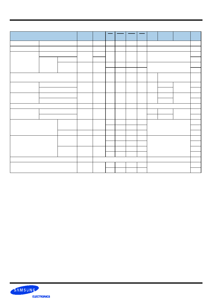
DDR SDRAM
128MB, 256MB Unbuffered SODIMM
Rev. 1.3 July 2005
(V=Valid, X=Don
′t Care, H=Logic High, L=Logic Low)
Note :
1. OP Code : Operand Code. A0 ~ A12 & BA0 ~ BA1 : Program keys. (@EMRS/MRS)
2. EMRS/ MRS can be issued only at all banks precharge state. A new command can be issued 2 clock cycles after EMRS or MRS.
3. Auto refresh functions are same as the CBR refresh of DRAM.
The automatical precharge without row precharge command is meant by "Auto".
Auto/self refresh can be issued only at all banks precharge state.
4. BA0 ~ BA1 : Bank select addresses.
If both BA0 and BA1 are "Low" at read, write, row active and precharge, bank A is selected.
If BA0 is "High" and BA1 is "Low" at read, write, row active and precharge, bank B is selected.
If BA0 is "Low" and BA1 is "High" at read, write, row active and precharge, bank C is selected.
If both BA0 and BA1 are "High" at read, write, row active and precharge, bank D is selected.
5. If A10/AP is "High" at row precharge, BA0 and BA1 are ignored and all banks are selected.
6. During burst write with auto precharge, new read/write command can not be issued.
Another bank read/write command can be issued after the end of burst.
New row active of the associated bank can be issued at tRP after the end of burst.
7. Burst stop command is valid at every burst length.
8. DM sampled at the rising and falling edges of the DQS and Data-in are masked at the both edges (Write DM latency is 0).
9. This combination is not defined for any function, which means "No Operation(NOP)" in DDR SDRAM.
COMMAND
CKEn-1
CKEn
CS
RAS
CAS
WE BA0,1 A10/AP
A0 ~ A9
A11, A12
Note
Register
Extended MRS
H
X
L
OP CODE
1, 2
Register
Mode Register Set
H
X
L
OP CODE
1, 2
Refresh
Auto Refresh
H
LL
L
H
X
3
Self
Refresh
Entry
L
3
Exit
L
H
LH
HH
X
3
HX
X
3
Bank Active & Row Addr.
H
X
L
H
V
Row Address
(A0~A9, A11,A12)
Read &
Column Address
Auto Precharge Disable
HX
L
H
L
H
V
L
Column
Address
4
Auto Precharge Enable
H
4
Write &
Column Address
Auto Precharge Disable
HX
L
H
L
V
L
Column
Address
4
Auto Precharge Enable
H
4, 6
Burst Stop
H
X
L
H
L
X
7
Precharge
Bank Selection
HX
L
H
L
VL
X
All Banks
X
H
5
Active Power Down
Entry
H
L
HX
X
LV
V
Exit
L
H
X
Precharge Power Down Mode
Entry
H
L
HX
X
LH
HH
Exit
L
H
HX
X
LV
V
DM
H
X
8
No operation (NOP) : Not defined
H
X
HX
X
9
LH
HH
9
16.0 Command Truth Table
相关PDF资料 |
PDF描述 |
|---|---|
| M470T2953CZ3-CE7 | 128M X 64 DDR DRAM MODULE, 0.4 ns, ZMA200 |
| M485L1624FT0-LA2 | 16M X 72 DDR DRAM MODULE, 0.75 ns, DMA200 |
| M485L1624FT0-CB3 | 16M X 72 DDR DRAM MODULE, 0.7 ns, DMA200 |
| M5-NP | UNSHIELDED, 0.056 uH - 0.12 uH, VARIABLE INDUCTOR, SMD |
| M504-7885022 | 50 CONTACT(S), MALE, RIGHT ANGLE PCMCIA CONNECTOR, SURFACE MOUNT |
相关代理商/技术参数 |
参数描述 |
|---|---|
| M470L3224FU0 | 制造商:SAMSUNG 制造商全称:Samsung semiconductor 功能描述:DDR SDRAM SODIMM |
| M470L3224FU0-CA2 | 制造商:SAMSUNG 制造商全称:Samsung semiconductor 功能描述:DDR SDRAM SODIMM |
| M470L3224FU0-CB0 | 制造商:SAMSUNG 制造商全称:Samsung semiconductor 功能描述:DDR SDRAM SODIMM |
| M470L3224FU0-CB3 | 制造商:SAMSUNG 制造商全称:Samsung semiconductor 功能描述:DDR SDRAM SODIMM |
| M470L3224HU0 | 制造商:SAMSUNG 制造商全称:Samsung semiconductor 功能描述:DDR SDRAM Product Guide |
发布紧急采购,3分钟左右您将得到回复。