- 您现在的位置:买卖IC网 > PDF目录359089 > M68AW128ML55ND6T (意法半导体) 2 Mbit (128K x16) 3.0V Asynchronous SRAM PDF资料下载
参数资料
| 型号: | M68AW128ML55ND6T |
| 厂商: | 意法半导体 |
| 英文描述: | 2 Mbit (128K x16) 3.0V Asynchronous SRAM |
| 中文描述: | 2兆位(128K的× 16)3.0V异步SRAM |
| 文件页数: | 8/22页 |
| 文件大小: | 335K |
| 代理商: | M68AW128ML55ND6T |
M68AW128M
8/22
OPERATION
The M68AW128M has a Chip Enable power down
feature which invokes an automatic standby mode
whenever either Chip Enable is de-asserted
(E = High) or LB and UB are de-asserted (LB and
UB = High). An Output Enable (G) signal provides
a high speed tri-state control, allowing fast read/
write cycles to be achieved with the common I/O
data bus. Operational modes are determined by
device control inputs W, E, LB and UB as summa-
rized in the Operating Modes table (see Table
2
).
Read Mode
The M68AW128M is in the Read mode whenever
Write Enable (W) is High with Output Enable (G)
Low, and Chip Enable (E) is asserted. This pro-
vides access to data from eight or sixteen, de-
pending on the status of the signal UB and LB, of
the 2,097,152 locations in the static memory array,
specified by the 17 address inputs. Valid data will
be available at the eight or sixteen output pins
within t
AVQV
after the last stable address, provid-
ing G is Low and E is Low. If Chip Enable or Output
Enable access times are not met, data access will
be measured from the limiting parameter (t
ELQV
,
t
GLQV
or t
BLQV
) rather than the address. Data out
may be indeterminate at t
ELQX
, t
GLQX
and t
BLQX
but data lines will always be valid at t
AVQV
.
Write Mode
The M68AW128M is in the Write mode whenever
the W and E are Low. Either the Chip Enable input
(E) or the Write Enable input (W) must be de-
asserted
during
Address
subsequent write cycles. When E (W) is Low, and
UB or LB is Low, write cycle begins on the W (E)'s
falling edge. When E and W are Low, and UB = LB
= High, write cycle begins on the first falling edge
of UB or LB. Therefore, address setup time is
referenced to Write Enable, Chip Enable or UB/LB
as t
AVWL
, t
AVEL
and t
AVBL
respectively, and is
determined by the latter occurring edge.
The Write cycle can be terminated by the earlier
rising edge of E, W or UB/LB.
If the Output is enabled (E = Low, G = Low, LB or
UB = Low), then W will return the outputs to high
impedance within t
WLQZ
of its falling edge. Care
must be taken to avoid bus contention in this type
of operation. Data input must be valid for t
DVWH
before the rising edge of Write Enable, or for t
DVEH
before the rising edge of E, or for t
DVBH
before the
transitions
for
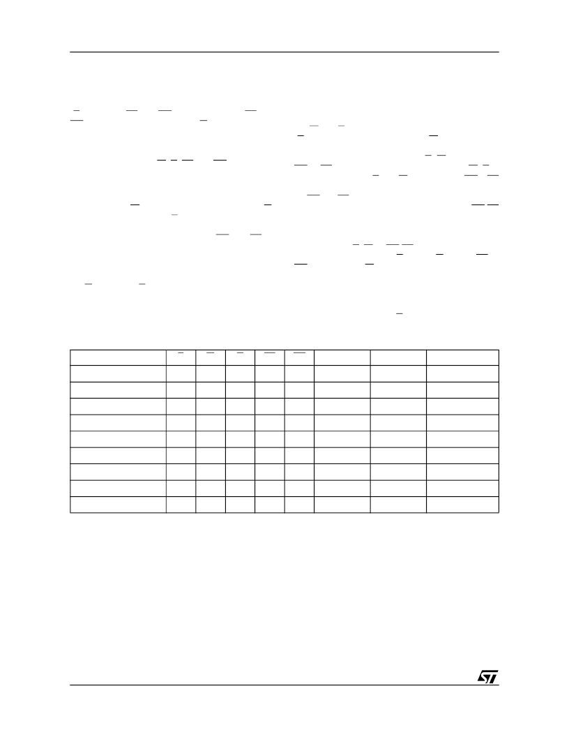
Table 2. Operating Modes
Note: 1. X = V
IH
or V
IL
.
Operation
E
W
G
LB
UB
DQ0-DQ7
DQ8-DQ15
Power
Deselected
V
IH
X
X
X
X
Hi-Z
Hi-Z
Standby (I
SB
)
Deselected
X
X
X
V
IH
V
IH
Hi-Z
Hi-Z
Standby (I
SB
)
Lower Byte Read
V
IL
V
IH
V
IL
V
IL
V
IH
Data Output
Hi-Z
Active (I
CC
)
Lower Byte Write
V
IL
V
IL
X
V
IL
V
IH
Data Input
Hi-Z
Active (I
CC
)
Output Disabled
V
IL
V
IH
V
IH
X
X
Hi-Z
Hi-Z
Active (I
CC
)
Upper Byte Read
V
IL
V
IH
V
IL
V
IH
V
IL
Hi-Z
Data Output
Active (I
CC
)
Upper Byte Write
V
IL
V
IL
X
V
IH
V
IL
Hi-Z
Data Input
Active (I
CC
)
Word Read
V
IL
V
IH
V
IL
V
IL
V
IL
Data Output
Data Output
Active (I
CC
)
Word Write
V
IL
V
IL
X
V
IL
V
IL
Data Input
Data Input
Active (I
CC
)
相关PDF资料 |
PDF描述 |
|---|---|
| M68AW128ML55ZB1 | 2 Mbit (128K x16) 3.0V Asynchronous SRAM |
| M68AW128ML55ZB1E | 2 Mbit (128K x16) 3.0V Asynchronous SRAM |
| M68AW128ML55ZB1F | 2 Mbit (128K x16) 3.0V Asynchronous SRAM |
| M68AW128ML55ZB1T | 2 Mbit (128K x16) 3.0V Asynchronous SRAM |
| M68AW128ML55ZB6 | 2 Mbit (128K x16) 3.0V Asynchronous SRAM |
相关代理商/技术参数 |
参数描述 |
|---|---|
| M68AW128ML55ZB1 | 制造商:STMICROELECTRONICS 制造商全称:STMicroelectronics 功能描述:2 Mbit (128K x16) 3.0V Asynchronous SRAM |
| M68AW128ML55ZB1E | 制造商:STMICROELECTRONICS 制造商全称:STMicroelectronics 功能描述:2 Mbit (128K x16) 3.0V Asynchronous SRAM |
| M68AW128ML55ZB1F | 制造商:STMICROELECTRONICS 制造商全称:STMicroelectronics 功能描述:2 Mbit (128K x16) 3.0V Asynchronous SRAM |
| M68AW128ML55ZB1T | 制造商:STMICROELECTRONICS 制造商全称:STMicroelectronics 功能描述:2 Mbit (128K x16) 3.0V Asynchronous SRAM |
| M68AW128ML55ZB6 | 制造商:STMICROELECTRONICS 制造商全称:STMicroelectronics 功能描述:2 Mbit (128K x16) 3.0V Asynchronous SRAM |
发布紧急采购,3分钟左右您将得到回复。