- 您现在的位置:买卖IC网 > PDF目录45052 > M8813F2W-15K1 (STMICROELECTRONICS) 128K X 8 FLASH, 27 I/O, PIA-GENERAL PURPOSE, PQCC52 PDF资料下载
参数资料
| 型号: | M8813F2W-15K1 |
| 厂商: | STMICROELECTRONICS |
| 元件分类: | 微控制器/微处理器 |
| 英文描述: | 128K X 8 FLASH, 27 I/O, PIA-GENERAL PURPOSE, PQCC52 |
| 封装: | PLASTIC, LCC-52 |
| 文件页数: | 10/85页 |
| 文件大小: | 601K |
| 代理商: | M8813F2W-15K1 |
第1页第2页第3页第4页第5页第6页第7页第8页第9页当前第10页第11页第12页第13页第14页第15页第16页第17页第18页第19页第20页第21页第22页第23页第24页第25页第26页第27页第28页第29页第30页第31页第32页第33页第34页第35页第36页第37页第38页第39页第40页第41页第42页第43页第44页第45页第46页第47页第48页第49页第50页第51页第52页第53页第54页第55页第56页第57页第58页第59页第60页第61页第62页第63页第64页第65页第66页第67页第68页第69页第70页第71页第72页第73页第74页第75页第76页第77页第78页第79页第80页第81页第82页第83页第84页第85页
M88 FAMILY
18/85
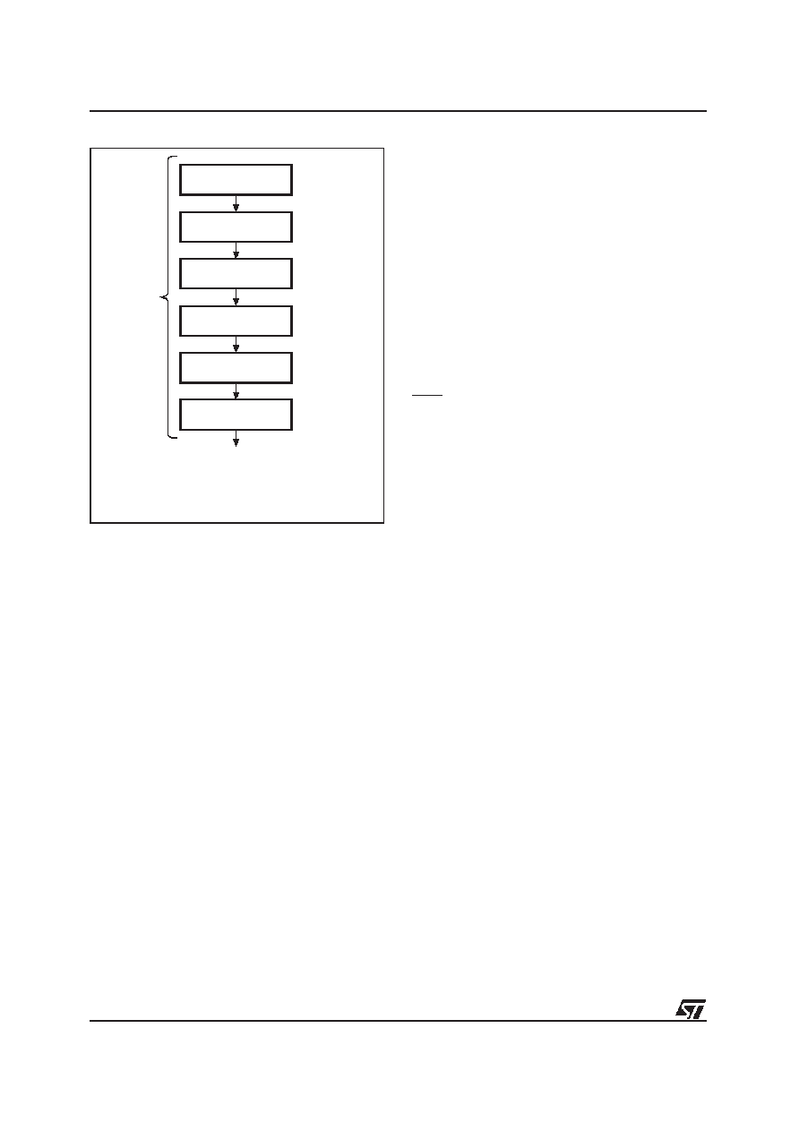
Figu re 6. EEPROM SDP-Disable Flowchart
AI01699C
Write AAh in
Address 5555h
Write 55h in
Address 2AAAh
Write 80h in
Address 5555h
Unprotected State
after
tWC (Write Cycle time)
Write AAh in
Address 5555h
Write 55h in
Address 2AAAh
Write 20h in
Address 5555h
Page Write
Timing
not supported when issuing the SDP enable or
SDP disable commands.
Using the SDP sequence (enabling, disabling, or
writing data) is initiated when specific bytes are
written to addresses on specific “pages” of
EEPROM memory, with no more than 120
s
between writes. The addresses 555h and AAAh
are located on different pages of EEPROM. This is
how the M88x3Fxx FLASH+PSD distinguishes
these instruction sequences from ordinary writes
to EEPROM, which are expected to be within a
single EEPROM page.
Write OTP Row (M8813F1x only)
Writing to the OTP row (64 bytes) can only be
done once, and is enabled by an instruction. This
instruction is composed of three specific Write
operations of data bytes at three specific memory
locations followed by the data to be stored in the
OTP row (refer to Table 11). During the write
operations, address bit A6 must be zero, while
address bits A5-A0 define the OTP Row byte to be
written while any EEPROM Sector Select signal
(EESi) is active. Writing the OTP row is allowed
only when the SDP mode is not enabled.
Programming Flash Memory
Flash memory must be erased prior to being
programmed. The MCU may erase Flash memory
all at once or by-sector, but not byte-by-byte. A
byte of Flash memory erases to all logic ones (FF
hex), and its bits are programmed to logic zeros.
Although erasing Flash memory occurs on a
sector basis, programming Flash memory occurs
on a byte basis.
The M88x3Fxx FLASH+PSD main Flash and
optional boot Flash require the MCU to send an
instruction to program a byte or perform an erase
function
(see
Table
11).
This
differs
from
EEPROM, which can be programmed with simple
MCU bus write operations (unless EEPROM SDP
mode is enabled).
Once the MCU issues a Flash memory program or
erase instruction, it must check for the status of
completion. The embedded algorithms that are
invoked
inside
the
M88x3Fxx
FLASH+PSD
support several means to provide status to the
MCU. Status may be checked using any of three
methods: Data Polling, Data Toggle, or the Ready/
Busy output pin.
Data Polling
Polling on DQ7 is a method of checking whether a
Program or Erase instruction is in progress or has
completed. Figure 7 shows the Data Polling
algorithm.
When the MCU issues a programming instruction,
the embedded algorithm within the M88x3Fxx
FLASH+PSD begins. The MCU then reads the
location of the byte to be programmed in Flash to
check status. Data bit DQ7 of this location
becomes the compliment of data bit 7of the
original data byte to be programmed. The MCU
continues to poll this location, comparing DQ7 and
monitoring the Error bit on DQ5. When the DQ7
matches data bit 7 of the original data, and the
Error bit at DQ5 remains ‘0’, then the embedded
algorithm is complete. If the Error bit at DQ5 is ‘1’,
the MCU should test DQ7 again since DQ7 may
have changed simultaneously with DQ5 (see
Figure 7).
The Error bit at DQ5 will be set if either an internal
time-out occurred while the embedded algorithm
attempted to program the byte or if the MCU
attempted to program a ‘1’ to a bit that was not
erased (not erased is logic ‘0’).
It is suggested (as with all Flash memories) to read
the
location
again
after
the
embedded
programming
algorithm
has
completed
to
compare the byte that was written to Flash with the
byte that was intended to be written.
When using the Data Polling method after an
erase instruction, Figure 7 still applies. However,
DQ7 will be ‘0’ until the erase operation is
complete. A ‘1’ on DQ5 will indicate a time-out
failure of the erase operation, a ‘0’ indicates no
error. The MCU can read any location within the
sector being erased to get DQ7 and DQ5.
相关PDF资料 |
PDF描述 |
|---|---|
| M8813F3W-15T1 | 1M X 1 FLASH, 27 I/O, PIA-GENERAL PURPOSE, PQFP52 |
| M8803F2Y-90T1 | 1M X 1 FLASH, 27 I/O, PIA-GENERAL PURPOSE, PQFP52 |
| M8803F3Y-90T1 | 1M X 1 FLASH, 27 I/O, PIA-GENERAL PURPOSE, PQFP52 |
| M8803F2Y-90T1T | 1M X 1 FLASH, 27 I/O, PIA-GENERAL PURPOSE, PQFP52 |
| M8803F3W-15K1 | 1M X 1 FLASH, 27 I/O, PIA-GENERAL PURPOSE, PQCC52 |
相关代理商/技术参数 |
参数描述 |
|---|---|
| M8813F2Y | 制造商:STMICROELECTRONICS 制造商全称:STMicroelectronics 功能描述:In-System Programmable ISP Multiple-Memory and Logic FLASHPSD Systems with CPLD for MCUs |
| M8813F2Y-90K6 | 制造商:STMicroelectronics 功能描述: |
| M88141W-15K1T | 制造商:STMICROELECTRONICS 制造商全称:STMicroelectronics 功能描述:In-System Programmable ISP Multiple-Memory and Logic FLASHPSD Systems with CPLD for MCUs |
| M88141W-15K6T | 制造商:STMICROELECTRONICS 制造商全称:STMicroelectronics 功能描述:In-System Programmable ISP Multiple-Memory and Logic FLASHPSD Systems with CPLD for MCUs |
| M88141W-15T1T | 制造商:STMICROELECTRONICS 制造商全称:STMicroelectronics 功能描述:In-System Programmable ISP Multiple-Memory and Logic FLASHPSD Systems with CPLD for MCUs |
发布紧急采购,3分钟左右您将得到回复。