- 您现在的位置:买卖IC网 > PDF目录45052 > M8813F2W-15K1 (STMICROELECTRONICS) 128K X 8 FLASH, 27 I/O, PIA-GENERAL PURPOSE, PQCC52 PDF资料下载
参数资料
| 型号: | M8813F2W-15K1 |
| 厂商: | STMICROELECTRONICS |
| 元件分类: | 微控制器/微处理器 |
| 英文描述: | 128K X 8 FLASH, 27 I/O, PIA-GENERAL PURPOSE, PQCC52 |
| 封装: | PLASTIC, LCC-52 |
| 文件页数: | 2/85页 |
| 文件大小: | 601K |
| 代理商: | M8813F2W-15K1 |
第1页当前第2页第3页第4页第5页第6页第7页第8页第9页第10页第11页第12页第13页第14页第15页第16页第17页第18页第19页第20页第21页第22页第23页第24页第25页第26页第27页第28页第29页第30页第31页第32页第33页第34页第35页第36页第37页第38页第39页第40页第41页第42页第43页第44页第45页第46页第47页第48页第49页第50页第51页第52页第53页第54页第55页第56页第57页第58页第59页第60页第61页第62页第63页第64页第65页第66页第67页第68页第69页第70页第71页第72页第73页第74页第75页第76页第77页第78页第79页第80页第81页第82页第83页第84页第85页
M88 FAMILY
10/85
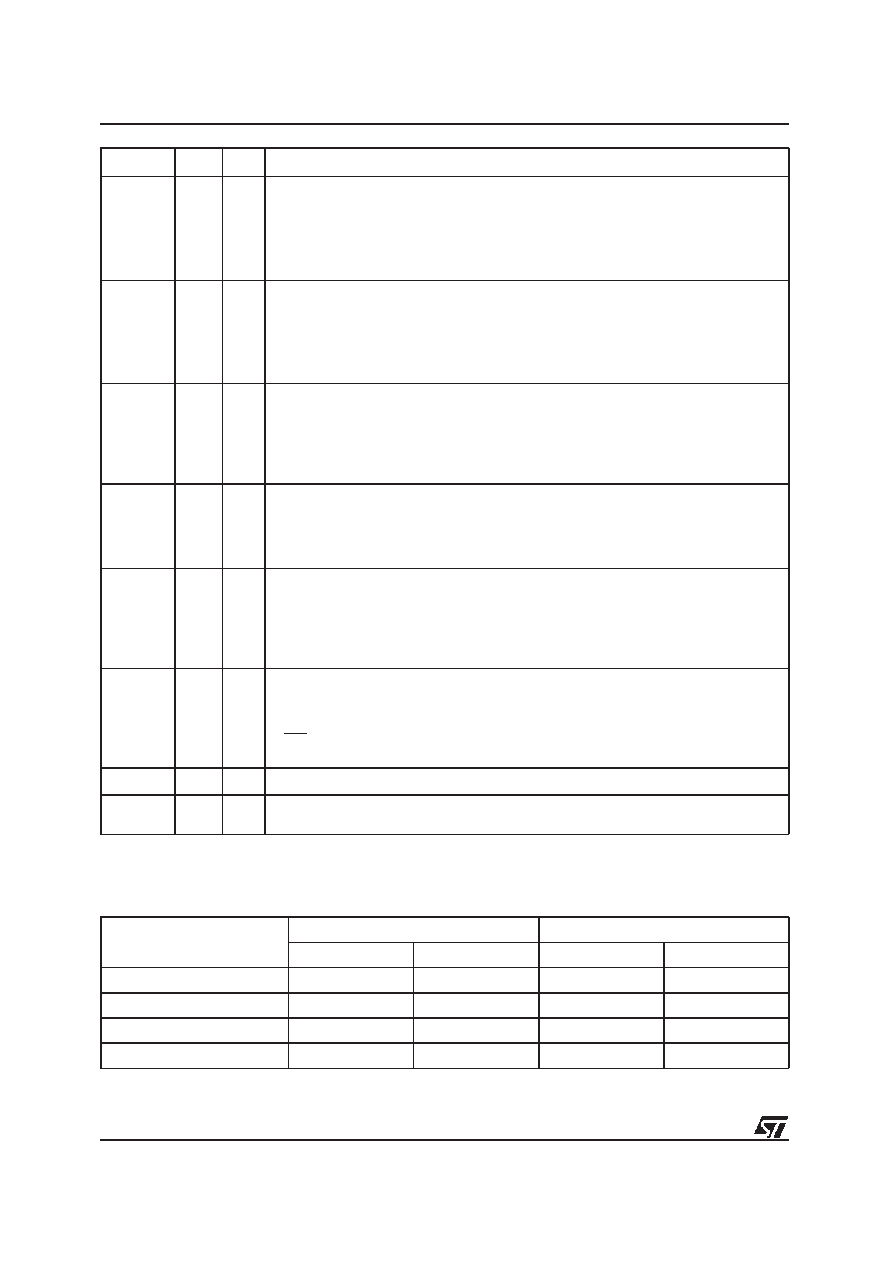
Note: 1. The pin numbers in this table are for the PLCC package only. See the package information, on page 79 onwards, for pin numbers
on other package types.
2. These functions can be multiplexed with other functions.
Table 8. I/O Port Latched Address Output Assignments1
Note: 1. Refer to the section entitled “I/O Ports”, on page 39, on how to enable the Latched Address Output function.
2. N/A = Not Applicable
PC5
13
I/O
PC5 pin of Port C. This port pin can be configured to have the following functions:
1. MCU I/O — write to or read from a standard output or input port.
2. CPLD Macrocell (McellBC5) output.
3. Input to the PLDs.
4. TDI input2 for the JTAG interface.
This pin can be configured as a CMOS or Open Drain output.
PC6
12
I/O
PC6 pin of Port C. This port pin can be configured to have the following functions:
1. MCU I/O — write to or read from a standard output or input port.
2. CPLD Macrocell (McellBC6) output.
3. Input to the PLDs.
4. TDO output2 for the JTAG interface.
This pin can be configured as a CMOS or Open Drain output.
PC7
11
I/O
PC7 pin of Port C. This port pin can be configured to have the following functions:
1. MCU I/O — write to or read from a standard output or input port.
2. CPLD Macrocell (McellBC7) output.
3. Input to the PLDs.
4. DBE — active-low Data Byte Enable input from 68HC912 type MCUs.
This pin can be configured as a CMOS or Open Drain output.
PD0
10
I/O
PD0 pin of Port D. This port pin can be configured to have the following functions:
1. ALE/AS input latches address output from the MCU.
2. MCU I/O — write or read from a standard output or input port.
3. Input to the PLDs.
4. CPLD output (external chip select).
PD1
9
I/O
PD1 pin of Port D. This port pin can be configured to have the following functions:
1. MCU I/O — write to or read from a standard output or input port.
2. Input to the PLDs.
3. CPLD output (external chip select).
4. CLKIN — clock input to the CPLD Macrocells, the automatic power-down unit’s power-
down counter, and the CPLD AND array.
PD2
8
I/O
PD2 pin of Port D. This port pin can be configured to have the following functions:
1. MCU I/O — write to or read from a standard output or input port.
2. Input to the PLDs.
3. CPLD output (external chip select).
4. CSI — chip select input. When low, the MCU can access the PSD memory and I/O.
When high, the PSD memory blocks are disabled to conserve power.
VCC
15, 38
Power pins
GND
1, 16,
26
Ground pins
Microcontroller
Port A
Port B
Port A (3:0)
Port A (7:4)
Port B (3:0)
Port B (7:4)
8051XA (8-bit)
N/A
Address [7:4]
Address [11:8]
N/A
80C251 (page mode)
N/A
Address [11:8]
Address [15:12]
All other 8-bit multiplexed
Address [3:0]
Address [7:4]
Address [3:0]
Address [7:4]
8-bit non-multiplexed bus
N/A
Address [3:0]
Address [7:4]
Pin Name
Pin1
Type
Description
相关PDF资料 |
PDF描述 |
|---|---|
| M8813F3W-15T1 | 1M X 1 FLASH, 27 I/O, PIA-GENERAL PURPOSE, PQFP52 |
| M8803F2Y-90T1 | 1M X 1 FLASH, 27 I/O, PIA-GENERAL PURPOSE, PQFP52 |
| M8803F3Y-90T1 | 1M X 1 FLASH, 27 I/O, PIA-GENERAL PURPOSE, PQFP52 |
| M8803F2Y-90T1T | 1M X 1 FLASH, 27 I/O, PIA-GENERAL PURPOSE, PQFP52 |
| M8803F3W-15K1 | 1M X 1 FLASH, 27 I/O, PIA-GENERAL PURPOSE, PQCC52 |
相关代理商/技术参数 |
参数描述 |
|---|---|
| M8813F2Y | 制造商:STMICROELECTRONICS 制造商全称:STMicroelectronics 功能描述:In-System Programmable ISP Multiple-Memory and Logic FLASHPSD Systems with CPLD for MCUs |
| M8813F2Y-90K6 | 制造商:STMicroelectronics 功能描述: |
| M88141W-15K1T | 制造商:STMICROELECTRONICS 制造商全称:STMicroelectronics 功能描述:In-System Programmable ISP Multiple-Memory and Logic FLASHPSD Systems with CPLD for MCUs |
| M88141W-15K6T | 制造商:STMICROELECTRONICS 制造商全称:STMicroelectronics 功能描述:In-System Programmable ISP Multiple-Memory and Logic FLASHPSD Systems with CPLD for MCUs |
| M88141W-15T1T | 制造商:STMICROELECTRONICS 制造商全称:STMicroelectronics 功能描述:In-System Programmable ISP Multiple-Memory and Logic FLASHPSD Systems with CPLD for MCUs |
发布紧急采购,3分钟左右您将得到回复。