- 您现在的位置:买卖IC网 > PDF目录359126 > MA838 (Zarlink Semiconductor Inc.) SINGLE PHASE PULSE WIDTH MODULATION WAVEFORM GENERATOR PDF资料下载
参数资料
| 型号: | MA838 |
| 厂商: | Zarlink Semiconductor Inc. |
| 英文描述: | SINGLE PHASE PULSE WIDTH MODULATION WAVEFORM GENERATOR |
| 中文描述: | 单相脉宽调制波形发生器 |
| 文件页数: | 7/13页 |
| 文件大小: | 314K |
| 代理商: | MA838 |
6
MA838
Initialisation Register Function
The 24-bit initialisation register contains parameters which,
under normal operation, will be defined during the power-up
sequence. These parameters are particular to the drive circuitry
used, and therefore changing these parameters during a PWM
cycle is not recommended. Information in this register should
only be modified while
RST
is active (i.e. low) so that the PWM
outputs are inhibited (low) during the updating process.
The parameters set in the initialisation register are as
follows:
Carrier frequency
Low carrier frequencies reduce switching losses whereas
high carrier frequencies increase waveform resolution and can
allow ultrasonic operation.
Power Frequency Range
This sets the maximum power frequency that can be carried
within the PWM output waveforms. This would normally be set
to a value to prevent the motor system being operated outside
its design parameters.
Pulse delay time ('underlap')
For each phase of the PWM cycle there are two control
signals, one for the top switch connected to the positive
inverter DC supply and one for the bottom switch connected to
the negative inverter DC supply. In theory, the states of these
two switches are always complementary. However, due to the
finite and non-equal turn-on and turn- off times of power
devices, it is desirable when changing the state of the output
pair, to provide a short delay time during which both outputs are
off in order to avoid a short circuit through the switching
elements.
Pulse deletion time
A pure PWM sequence produces pulses which can vary in
width between 0% and 100% of the duty cycle. Therefore, in
theory, pulse widths can become infinitesimally narrow. In
practice this causes problems in the power switches due to
storage effects and therefore a minimum pulse width time is
required. All pulses shorter than the minimum specified are
deleted.
Counter reset
This facility allows the internal power frequency counter of
the MA838 to be set to zero, disabling the normal frequency
control and giving a 50% output duty cycle.
Initialisation Register Programming
The initialisation register data is loaded in 8-bit segments into
the three 8-bit temporary registers R0-R2. When all the initialisation
data has been loaded into these registers it is transferred into the
24-bit initialisation register by writing to the dummy register R4.
Carrier frequency selection
The carrier frequency is a function of the externally applied
clock frequency and a division ratio
n
, determined by the 3-bit
CFS word set during initialisation. The values of
n
are selected
as shown in Table 4.
The carrier frequency,
f
CARR
,
is then given by:
where
k
= clock frequency and
n
= 1, 2, 4, 8, 16 or 32 (as set
by FRS)
Power frequency range selection
The power frequency range selected here defines the maximum
limit of the power frequency. The operating power frequency is
controlled by the 12-bit Power Frequency Select (PFS) word in the
control register but may not exceed the value set here.
The power frequency range is a function of the carrier
waveform frequency (
f
) and a multiplication factor
m
,
determined by the 3-bit FRS word. The value of
m
is determined
as shown in Table 5.
Pulse delay time
The pulse delay time affects all six PWM outputs by delaying
the rising edges of each of the outputs by an equal amount.
The pulse delay time is a function of the carrier waveform
frequency and
pdy
, defined by the 6-bit pulse delay time select
word (PDY). The value of
pdy
is selected as shown in Table 6.
The pulse delay time,
t
pdy
, is then given by:
where
pdy
= 1- 64 (as set by PDY) and
f
CARR
= carrier
frequency.
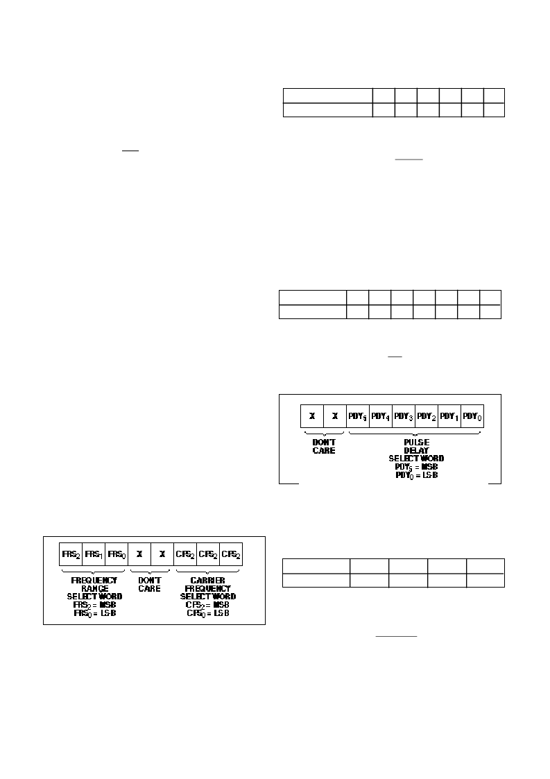
Fig. 6 Temporary register R1
CFS word
Value of n
Table 4 Values of clock division ratio n
000
1
001
2
010
4
011
8
100
16
101
32
f
CARR
=
k
512
x
n
FRS word
Value of m
Table 5 Values of carrier frequency multiplicaion factor m
The power frequency range,
f
RANGE
, is then given by:
f
CARR
384
000
1
001
2
010
4
011
8
100
16
101
32
110
64
where
f
= carrier frequency and
m
= 1, 2, 4, 8, 16, 32 or
64 (as set by FRS).
f
RANGE
=
x
m
Fig. 7 Temporary register R2
PDY word
Value of pdy
000000
64
...etc...
...etc...
111110
2
Table 6 Values of pdy
111111
1
t
pdy
=
pdy
f
CARR
x 512
相关PDF资料 |
PDF描述 |
|---|---|
| MAADSS0010 | Digital Attenuator, 5-Bit, 31 dB (400 - 2500 MHz) |
| MAAL-007673 | Low Noise Amplifier 1.7 - 2.0 GHz |
| MAAL-008091 | High Dynamic Range Low Noise Amplifier 800 - 1000 MHz |
| MAALSS0012 | Miniature Broadband Gain Stage 200 - 3000 MHz |
| MAALSS0012-3000 | Circular Connector; MIL SPEC:MIL-C-5015; Body Material:Metal; Series:GT; No. of Contacts:2; Connector Shell Size:32; Connecting Termination:Solder; Circular Shell Style:Square Flange Receptacle; Body Style:Straight |
相关代理商/技术参数 |
参数描述 |
|---|---|
| MA8390 | 制造商:PANASONIC 制造商全称:Panasonic Semiconductor 功能描述:Silicon planar type |
| MA83900H | 制造商:PANASONIC 制造商全称:Panasonic Semiconductor 功能描述:Silicon planar type |
| MA83900L | 制造商:PANASONIC 制造商全称:Panasonic Semiconductor 功能描述:Silicon planar type |
| MA83900M | 制造商:PANASONIC 制造商全称:Panasonic Semiconductor 功能描述:Silicon planar type |
| MA840 | 制造商:PANASONIC 制造商全称:Panasonic Semiconductor 功能描述:Variable Capacitance Diodes |
发布紧急采购,3分钟左右您将得到回复。