- 您现在的位置:买卖IC网 > PDF目录18824 > MAX1005CEE+ (Maxim Integrated)IC UNDERSAMPLER IF 16-QSOP PDF资料下载
参数资料
| 型号: | MAX1005CEE+ |
| 厂商: | Maxim Integrated |
| 文件页数: | 8/8页 |
| 文件大小: | 0K |
| 描述: | IC UNDERSAMPLER IF 16-QSOP |
| 产品培训模块: | Lead (SnPb) Finish for COTS Obsolescence Mitigation Program |
| 标准包装: | 100 |
| 功能: | IF 欠采样器 |
| RF 型: | PCS,PHS,WLL |
| 次要属性: | 并行逻辑接口 |
| 封装/外壳: | 16-SSOP(0.154",3.90mm 宽) |
| 包装: | 管件 |
�� �
�
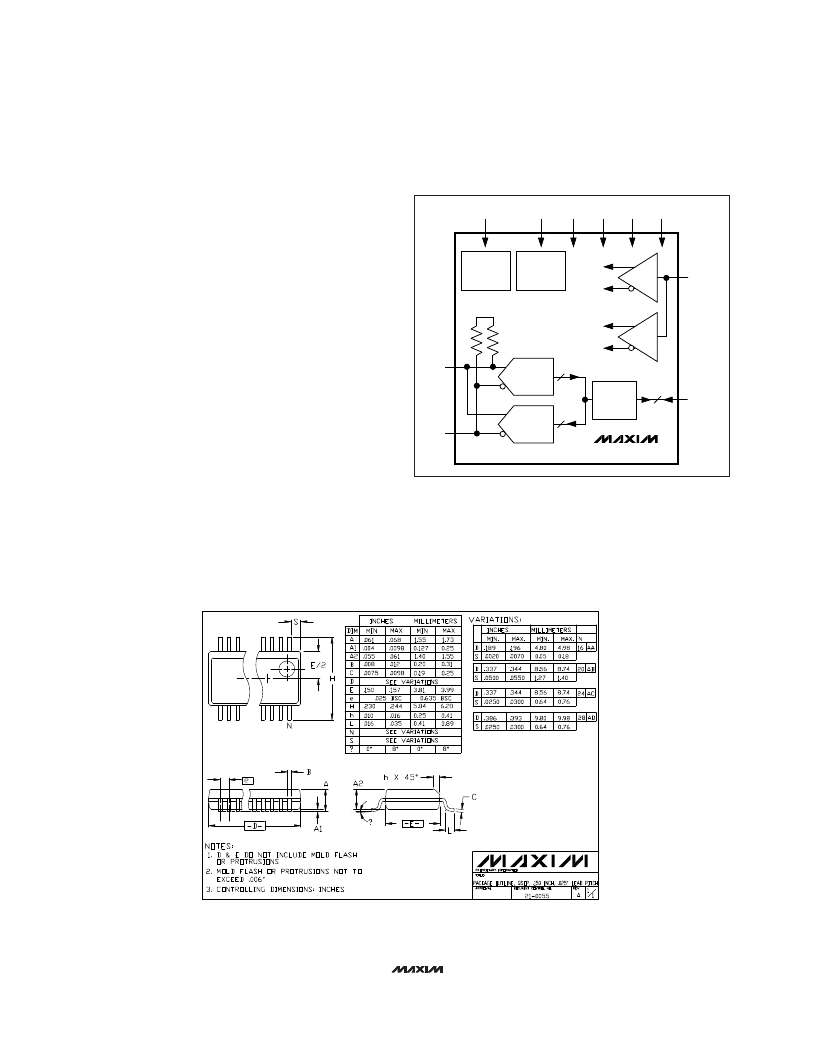
�IF� Undersampler�
�Power-Supply� Bypassing� and� Grounding�
�The� MAX1005� has� separate� analog� (VCCA)� and� digital�
�________________Functional� Diagram�
�(VCCD)� power-supply� connections,� as� well� as� separate�
�analog� and� digital� ground� connections� to� minimize� cou-�
�TXEN�
�RXEN�
�VCCA�
�AGND�
�VCCD�
�DGND�
�pling� of� noisy� digital� signals� into� the� circuit’s� analog� por-�
�tion.� The� device� will� operate� with� both� of� these� power�
�supplies� connected� to� any� voltage� between� +2.7V� and�
�+5.5V.� This� feature� allows� the� digital� circuitry� to� operate�
�from� a� regulated� logic� power� supply;� this� reduces� power�
�DAC�
�BANDGAP�
�REFERENCE�
�ADC�
�BANDGAP�
�REFERENCE�
�ADC�
�CLOCK�
�DRIVER�
�CLK�
�consumption� and� maintains� compatibility� with� external�
�logic,� while� allowing� the� analog� circuitry� to� operate� from�
�an� unregulated� supply.�
�The� analog� ground� (AGND)� and� digital� ground� (DGND)�
�should� be� tied� together� close� to� the� device.� At� no� time�
�should� the� voltage� between� AGND� and� DGND� exceed�
�AIO+�
�1k�
�VCCA�
�1k�
�5-BIT�
�FLASH� ADC�
�5�
�DAC�
�CLOCK�
�DRIVER�
�±0.3V.�
�The� entire� board� needs� good� DC� bypassing� for� both�
�analog� and� digital� supplies.� Place� the� power-supply�
�bypass� capacitors� close� to� where� the� power� is� routed�
�onto� board.� 10μF� electrolytic� capacitors� with� low� equiva-�
�AIO-�
�7-BIT� DAC�
�7�
�DIGITAL�
�INTERFACE�
�MAX1005�
�7�
�D6–D0�
�lent-series-resistance� (ESR)� ratings� are� recommended.�
�For� best� effective� bits� performance,� minimize� capacitive�
�loading� at� the� digital� outputs.� Keep� the� digital� output�
�traces� as� short� as� possible.� Bypass� each� of� the� VCC_�
�supply� pins� to� its� respective� GND� with� high-quality�
�ceramic� capacitors� located� as� close� to� the� package� as�
�possible.�
�___________________Chip� Information�
�TRANSISTOR� COUNT:� 2377�
�SUBSTRATE� CONNECTED� TO� AGND�
�________________________________________________________Package� Information�
�Maxim� cannot� assume� responsibility� for� use� of� any� circuitry� other� than� circuitry� entirely� embodied� in� a� Maxim� product.� No� circuit� patent� licenses� are�
�implied.� Maxim� reserves� the� right� to� change� the� circuitry� and� specifications� without� notice� at� any� time.�
�8� _____________________Maxim� Integrated� Products,� 120� San� Gabriel� Drive,� Sunnyvale,� CA� 94086� 408-737-7600�
�?� 1997� Maxim� Integrated� Products�
�Printed� USA�
�is� a� registered� trademark� of� Maxim� Integrated� Products.�
�相关PDF资料 |
PDF描述 |
|---|---|
| 6576-60-0 | CORD ALLIG-ALLIG W/BOOT 60" BLK |
| 104M06QC150 | SUPP RC NETWORK .10UF 150OHM |
| 6576-48-2 | CORD ALLIG-ALLIG W/BOOT 48" RED |
| CD631215B | SCR MOD DUAL 1200V 150A |
| CD631015B | SCR MOD DUAL 1000V 150A |
相关代理商/技术参数 |
参数描述 |
|---|---|
| MAX1005CEE+ | 功能描述:射频无线杂项 IF Undersampler RoHS:否 制造商:Texas Instruments 工作频率:112 kHz to 205 kHz 电源电压-最大:3.6 V 电源电压-最小:3 V 电源电流:8 mA 最大功率耗散: 工作温度范围:- 40 C to + 110 C 封装 / 箱体:VQFN-48 封装:Reel |
| MAX1005CEE+T | 功能描述:射频无线杂项 IF Undersampler RoHS:否 制造商:Texas Instruments 工作频率:112 kHz to 205 kHz 电源电压-最大:3.6 V 电源电压-最小:3 V 电源电流:8 mA 最大功率耗散: 工作温度范围:- 40 C to + 110 C 封装 / 箱体:VQFN-48 封装:Reel |
| MAX1005CEE-T | 功能描述:射频无线杂项 RoHS:否 制造商:Texas Instruments 工作频率:112 kHz to 205 kHz 电源电压-最大:3.6 V 电源电压-最小:3 V 电源电流:8 mA 最大功率耗散: 工作温度范围:- 40 C to + 110 C 封装 / 箱体:VQFN-48 封装:Reel |
| MAX1005EEE | 功能描述:射频无线杂项 RoHS:否 制造商:Texas Instruments 工作频率:112 kHz to 205 kHz 电源电压-最大:3.6 V 电源电压-最小:3 V 电源电流:8 mA 最大功率耗散: 工作温度范围:- 40 C to + 110 C 封装 / 箱体:VQFN-48 封装:Reel |
| MAX1005EEE+ | 功能描述:射频无线杂项 IF Undersampler RoHS:否 制造商:Texas Instruments 工作频率:112 kHz to 205 kHz 电源电压-最大:3.6 V 电源电压-最小:3 V 电源电流:8 mA 最大功率耗散: 工作温度范围:- 40 C to + 110 C 封装 / 箱体:VQFN-48 封装:Reel |
发布紧急采购,3分钟左右您将得到回复。