- 您现在的位置:买卖IC网 > PDF目录1935 > MAX1042BETX+ (Maxim Integrated Products)IC ADC/DAC 10BIT W/FIFO 36TQFN PDF资料下载
参数资料
| 型号: | MAX1042BETX+ |
| 厂商: | Maxim Integrated Products |
| 文件页数: | 9/39页 |
| 文件大小: | 0K |
| 描述: | IC ADC/DAC 10BIT W/FIFO 36TQFN |
| 产品培训模块: | Lead (SnPb) Finish for COTS Obsolescence Mitigation Program |
| 标准包装: | 50 |
| 类型: | ADC,DAC |
| 分辨率(位): | 10 b |
| 采样率(每秒): | 225k |
| 数据接口: | DSP,MICROWIRE?,QSPI?,串行,SPI? |
| 电压电源: | 模拟和数字 |
| 电源电压: | 4.75 V ~ 5.25 V |
| 工作温度: | -40°C ~ 85°C |
| 安装类型: | 表面贴装 |
| 封装/外壳: | 36-WFQFN 裸露焊盘 |
| 供应商设备封装: | 36-TQFN 裸露焊盘(6x6) |
| 包装: | 管件 |
第1页第2页第3页第4页第5页第6页第7页第8页当前第9页第10页第11页第12页第13页第14页第15页第16页第17页第18页第19页第20页第21页第22页第23页第24页第25页第26页第27页第28页第29页第30页第31页第32页第33页第34页第35页第36页第37页第38页第39页
MAX1040/MAX1042/MAX1046/MAX1048
10-Bit, Multichannel ADCs/DACs with FIFO,
Temperature Sensing, and GPIO Ports
______________________________________________________________________________________
17
Unipolar or Bipolar Conversions
Address the unipolar- and bipolar-mode registers
through the setup register (bits 1 and 0). See Table 5 for
the setup register. See Figures 3 and 4 for the transfer-
function graphs. Program a pair of analog inputs for dif-
ferential operation by writing a one to the appropriate bit
of the bipolar- or unipolar-mode register. Unipolar mode
sets the differential input range from 0 to VREF1. A nega-
tive differential analog input in unipolar mode causes the
digital output code to be zero. Selecting bipolar mode
sets the differential input range to ±VREF1 / 2. The digital
output code is binary in unipolar mode and two’s com-
plement in bipolar mode.
In single-ended mode, the MAX1040/MAX1042/
MAX1046/MAX1048 always operate in unipolar mode.
The analog inputs are internally referenced to AGND
with a full-scale input range from 0 to the selected refer-
ence voltage.
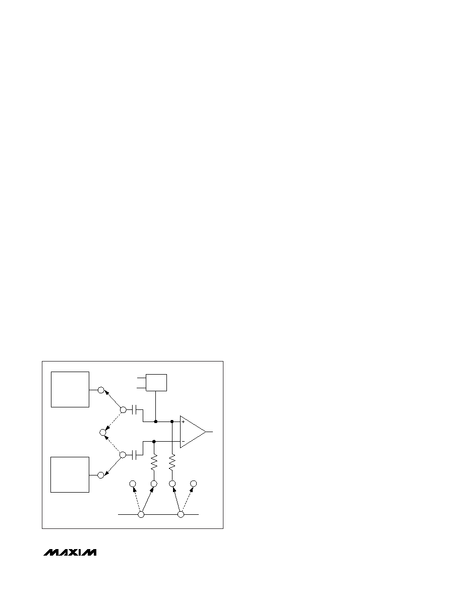
Analog Input (T/H)
The equivalent circuit of Figure 2 shows the ADC input
architecture of the MAX1040/MAX1042/MAX1046/
MAX1048. In track mode, a positive input capacitor is
connected to AIN0–AIN7 in single-ended mode and
AIN0, AIN2, AIN4, and AIN6 in differential mode.
A negative input capacitor is connected to AGND in
single-ended mode or AIN1, AIN3, AIN5, and AIN7 in
differential mode. For external T/H timing, use clock
mode 01. After the T/H enters hold mode, the difference
between the sampled positive and negative input volt-
ages is converted. The input capacitance charging rate
determines the time required for the T/H to acquire an
input signal. If the input signal’s source impedance is
high, the required acquisition time lengthens.
Any source impedance below 300Ω does not signifi-
cantly affect the ADC’s AC performance. A high-imped-
ance source can be accommodated either by
lengthening tACQ (only in clock mode 01) or by placing
a 1F capacitor between the positive and negative ana-
log inputs. The combination of the analog-input source
impedance and the capacitance at the analog input cre-
ates an RC filter that limits the analog input bandwidth.
Input Bandwidth
The ADC’s input-tracking circuitry has a 1MHz small-sig-
nal bandwidth, making it possible to digitize high-speed
transient events and measure periodic signals with
bandwidths exceeding the ADC’s sampling rate by
using undersampling techniques. Anti-alias prefiltering
of the input signals is necessary to avoid high-frequency
signals aliasing into the frequency band of interest.
Analog Input Protection
Internal electrostatic-discharge (ESD) protection diodes
clamp all analog inputs to AVDD and AGND, allowing
the inputs to swing from (AGND - 0.3V) to (AVDD +
0.3V) without damage. However, for accurate conver-
sions near full scale, the inputs must not exceed AVDD
by more than 50mV or be lower than AGND by 50mV. If
an analog input voltage exceeds the supplies, limit the
input current to 2mA.
Internal FIFO
The MAX1040/MAX1042/MAX1046/MAX1048 contain a
first-in/first-out (FIFO) buffer that holds up to 16 ADC
results plus one temperature result. The internal FIFO
allows the ADC to process and store multiple internally
clocked conversions and a temperature measurement
without being serviced by the serial bus.
If the FIFO is filled and further conversions are request-
ed without reading from the FIFO, the oldest ADC
results are overwritten by the new ADC results. Each
result contains 2 bytes, with the MSB preceded by four
leading zeros. After each falling edge of
CS, the oldest
available pair of bytes of data is available at DOUT,
MSB first. When the FIFO is empty, DOUT is zero.
The first 2 bytes of data read out after a temperature
measurement always contain the 10-bit temperature
result, preceded by four leading zeros, MSB first. The
LSB is followed by 2 sub-bits. If another temperature
measurement is performed before the first temperature
result is read out, the old measurement is overwritten
by the new result. Temperature results are in degrees
AIN0–AIN7
(SINGLE-ENDED),
AIN0, AIN2,
AIN4, AIN6
(DIFFERENTIAL)
COMPARATOR
HOLD
ACQ
HOLD
ACQ
HOLD
AVDD / 2
REF1
AGND
CIN+
CIN-
DAC
AGND
(SINGLE-ENDED),
AIN1, AIN3,
AIN5, AIN7
(DIFFERENTIAL)
Figure 2. Equivalent Input Circuit
相关PDF资料 |
PDF描述 |
|---|---|
| MAX1057BETM+T | IC ADC/DAC 10BIT 48-TQFN-EP |
| MAX11041ETC+T | IC REMOTE CTRLR WIRED 12-TQFN |
| MAX11043ATL+T | IC ADC 16BIT W/DAC 40-TQFN-EP |
| MAX11359AETL+T | IC DAS SYSTEM 16BIT 40-TQFN |
| MAX115CAX+ | IC DAS SYSTEM 12BIT 36-SSOP |
相关代理商/技术参数 |
参数描述 |
|---|---|
| MAX1042BETX+ | 功能描述:ADC / DAC多通道 10Bit AD/DACs w/FIFO Temp Sns & GPIO Port RoHS:否 制造商:Texas Instruments 转换速率: 分辨率:8 bit 接口类型:SPI 电压参考: 电源电压-最大:3.6 V 电源电压-最小:2 V 最大工作温度:+ 85 C 安装风格:SMD/SMT 封装 / 箱体:VQFN-40 |
| MAX1042BETX+T | 功能描述:ADC / DAC多通道 10Bit AD/DACs w/FIFO Temp Sns & GPIO Port RoHS:否 制造商:Texas Instruments 转换速率: 分辨率:8 bit 接口类型:SPI 电压参考: 电源电压-最大:3.6 V 电源电压-最小:2 V 最大工作温度:+ 85 C 安装风格:SMD/SMT 封装 / 箱体:VQFN-40 |
| MAX1042BETX-T | 功能描述:ADC / DAC多通道 RoHS:否 制造商:Texas Instruments 转换速率: 分辨率:8 bit 接口类型:SPI 电压参考: 电源电压-最大:3.6 V 电源电压-最小:2 V 最大工作温度:+ 85 C 安装风格:SMD/SMT 封装 / 箱体:VQFN-40 |
| MAX1043 | 制造商:MAXIM 制造商全称:Maxim Integrated Products 功能描述:10-Bit, Multichannel ADCs/DACs with FIFO, Temperature Sensing, and GPIO Ports |
| MAX1043BETX | 功能描述:ADC / DAC多通道 RoHS:否 制造商:Texas Instruments 转换速率: 分辨率:8 bit 接口类型:SPI 电压参考: 电源电压-最大:3.6 V 电源电压-最小:2 V 最大工作温度:+ 85 C 安装风格:SMD/SMT 封装 / 箱体:VQFN-40 |
发布紧急采购,3分钟左右您将得到回复。