- 您现在的位置:买卖IC网 > PDF目录9975 > MAX11665AUT+T (Maxim Integrated Products)ADC 12BIT 500KSPS 1CH SOT23-6 PDF资料下载
参数资料
| 型号: | MAX11665AUT+T |
| 厂商: | Maxim Integrated Products |
| 文件页数: | 13/28页 |
| 文件大小: | 0K |
| 描述: | ADC 12BIT 500KSPS 1CH SOT23-6 |
| 产品培训模块: | Lead (SnPb) Finish for COTS Obsolescence Mitigation Program |
| 标准包装: | 2,500 |
| 位数: | 12 |
| 采样率(每秒): | 500k |
| 数据接口: | MICROWIRE?,QSPI?,串行,SPI? |
| 转换器数目: | 1 |
| 功率耗散(最大): | 696mW |
| 电压电源: | 模拟和数字 |
| 工作温度: | -40°C ~ 125°C |
| 安装类型: | 表面贴装 |
| 封装/外壳: | SOT-23-6 |
| 供应商设备封装: | SOT-23-6 |
| 包装: | 带卷 (TR) |
| 输入数目和类型: | 1 个单端,单极 |
第1页第2页第3页第4页第5页第6页第7页第8页第9页第10页第11页第12页当前第13页第14页第15页第16页第17页第18页第19页第20页第21页第22页第23页第24页第25页第26页第27页第28页
20 _____________________________________________________________________________________
MAX11661–MAX11666
500ksps, Low-Power,
Serial 12-/10-/8-Bit ADCs
Detailed Description
The MAX11661–MAX11666 are fast, 12-/10-/8-bit, low-
power, single-supply ADCs. The devices operate from
a 2.2V to 3.6V supply and consume only 2.98mW
(VDD = 2.2V) or 4.37mW (VDD = 3V). These devices
are capable of sampling at full rate when driven by
an 8MHz clock. The dual-channel devices provide a
separate digital supply input (OVDD) to power the digi-
tal interface enabling communication with 1.5V, 1.8V,
2.5V, or 3V digital systems.
The conversion result appears at DOUT, MSB first, with a
leading zero followed by the 12-bit, 10-bit, or 8-bit result.
A 12-bit result is followed by two trailing zeros, a 10-bit
result is followed by four trailing zeros, and an 8-bit result
is followed by six trailing zeros. See Figures 1 and 5.
The dual-channel devices feature a dedicated refer-
ence input (REF). The input signal range for AIN1/AIN2
is defined as 0V to VREF with respect to AGND. The
single-channel devices use VDD as the reference. The
input signal range of AIN is defined as 0V to VDD with
respect to GND.
These ADCs include a power-down feature allowing
minimized power consumption at 2.5FA/ksps for lower
throughput rates. The wake-up and power-down feature
is controlled by using the SPI interface as described in
the Operating Modes section.
Serial Interface
The devices feature a 3-wire serial interface that directly
connects to SPI, QSPI, and MICROWIRE devices without
external logic. Figures 1 and 5 show the interface sig-
nals for a single conversion frame to achieve maximum
throughput.
The falling edge of CS defines the sampling instant.
Once CS transitions low, the external clock signal
(SCLK) controls the conversion.
The SAR core successively extracts binary-weighted bits
in every clock cycle. The MSB appears on the data bus
during the 2nd clock cycle with a delay outlined in the
timing specifications. All extracted data bits appear suc-
cessively on the data bus with the LSB appearing during
the 13th/11th/9th clock cycle for 12-/10-/8-bit operation.
The serial data stream of conversion bits is preceded by
a leading “zero” and succeeded by trailing “zeros.” The
data output (DOUT) goes into a high-impedance state
during the 16th clock cycle.
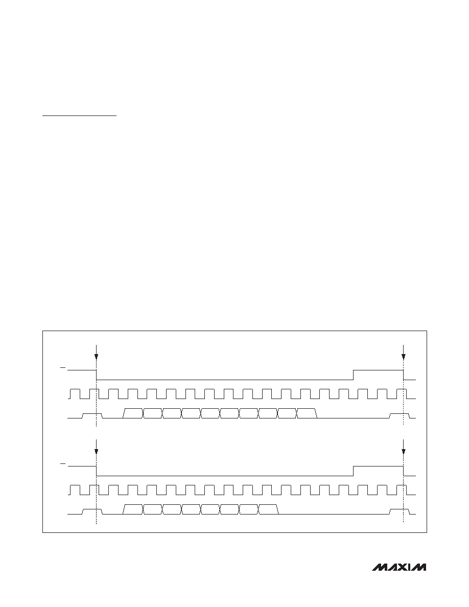
Figure 5. 10-/8-Bit Timing Diagrams
SCLK
12
3
45
67
89
10
11
12
13
14
15
16
1
SAMPLE
CS
DOUT
HIGH
IMPEDANCE
HIGH
IMPEDANCE
HIGH
IMPEDANCE
HIGH
IMPEDANCE
0
00
D9
D8
D7
D6
D5
D4
D3
D2
D1
D0
00
SAMPLE
SCLK
CS
12
3
45
67
89
10
11
12
13
14
15
16
1
DOUT
0
00
D7
D6
D5
D4
D3
D2
D1
D0
00
相关PDF资料 |
PDF描述 |
|---|---|
| MS27473T16F8PA | CONN PLUG 8POS STRAIGHT W/PINS |
| MS27473T18A35SB | CONN PLUG 66POS STRAIGHT W/SCKT |
| IDT72265LA10TFG8 | IC FIFO 8KX18 LP 10NS 64QFP |
| MS27499E14A35SA | CONN RCPT 37POS BOX MNT W/SCKT |
| IDT72265LA10TF8 | IC FIFO 8KX18 LP 10NS 64QFP |
相关代理商/技术参数 |
参数描述 |
|---|---|
| MAX11665EVKIT# | 功能描述:数据转换 IC 开发工具 MAX11665 Eval Kit RoHS:否 制造商:Texas Instruments 产品:Demonstration Kits 类型:ADC 工具用于评估:ADS130E08 接口类型:SPI 工作电源电压:- 6 V to + 6 V |
| MAX11666 | 制造商:MAXIM 制造商全称:Maxim Integrated Products 功能描述:500ksps, Low-Power,Serial 12-/10-/8-Bit ADCs |
| MAX11666AUB | 制造商:MAXIM 制造商全称:Maxim Integrated Products 功能描述:500ksps, Low-Power,Serial 12-/10-/8-Bit ADCs |
| MAX11666AUB/V | 制造商:MAXIM 制造商全称:Maxim Integrated Products 功能描述:500ksps, Low-Power,Serial 12-/10-/8-Bit ADCs |
| MAX11666AUB/V+ | 功能描述:模数转换器 - ADC 1-2Ch 12-Bit 500ksps ADC RoHS:否 制造商:Texas Instruments 通道数量:2 结构:Sigma-Delta 转换速率:125 SPs to 8 KSPs 分辨率:24 bit 输入类型:Differential 信噪比:107 dB 接口类型:SPI 工作电源电压:1.7 V to 3.6 V, 2.7 V to 5.25 V 最大工作温度:+ 85 C 安装风格:SMD/SMT 封装 / 箱体:VQFN-32 |
发布紧急采购,3分钟左右您将得到回复。