- 您现在的位置:买卖IC网 > PDF目录10487 > MAX1400EAI+ (Maxim Integrated Products)IC ADC 18BIT LP 28-SSOP PDF资料下载
参数资料
| 型号: | MAX1400EAI+ |
| 厂商: | Maxim Integrated Products |
| 文件页数: | 19/34页 |
| 文件大小: | 0K |
| 描述: | IC ADC 18BIT LP 28-SSOP |
| 产品培训模块: | MAX11200 ADC Lead (SnPb) Finish for COTS Obsolescence Mitigation Program |
| 标准包装: | 46 |
| 位数: | 18 |
| 采样率(每秒): | 480 |
| 数据接口: | QSPI?,串行,SPI? |
| 转换器数目: | 1 |
| 功率耗散(最大): | 1.25mW |
| 电压电源: | 模拟和数字 |
| 工作温度: | -40°C ~ 85°C |
| 安装类型: | 表面贴装 |
| 封装/外壳: | 28-SSOP(0.209",5.30mm 宽) |
| 供应商设备封装: | 28-SSOP |
| 包装: | 管件 |
| 输入数目和类型: | 3 个差分,单极;3 个差分,双极;5 个伪差分,单极;5 个伪差分,双极 |
| 产品目录页面: | 1396 (CN2011-ZH PDF) |
第1页第2页第3页第4页第5页第6页第7页第8页第9页第10页第11页第12页第13页第14页第15页第16页第17页第18页当前第19页第20页第21页第22页第23页第24页第25页第26页第27页第28页第29页第30页第31页第32页第33页第34页
MAX1400
+5V, 18-Bit, Low-Power, Multichannel,
Oversampling (Sigma-Delta) ADC
26
______________________________________________________________________________________
The noise shown in Table 16 is composed of device noise
and quantization noise. The device noise is relatively low
but becomes the limiting noise source for high gain set-
tings. The quantization noise is determined by the notch
frequency and becomes the dominant noise source as the
notch frequency is increased.
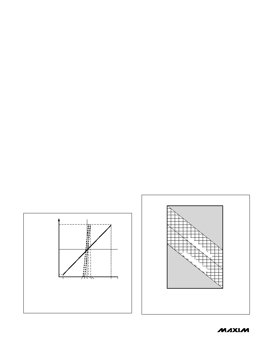
Offset Correction DAC
The MAX1400 provides a coarse (3-bit plus sign) offset
correction DAC at the modulator input. Use this DAC to
remove the offset component in the input signal, allowing
the ADC to operate on a more sensitive range. The DAC
offsets up to ±116.7% of the selected range in ±16.7%
increments for unipolar mode and up to ±58.3% of the
selected range in ±8.3% increments for bipolar mode.
When a DAC value of 0 is selected, the DAC is completely
disconnected from the modulator inputs and does not
contribute any noise. Figures 8 and 9 show the effect of
the DAC codes on the input range and transfer function.
Clock Oscillator
The clock oscillator may be used with an external crystal
(or resonator) connected between CLKIN and CLKOUT,
or may be driven directly by an external oscillator at
CLKIN with CLKOUT left unconnected. In normal oper-
ating mode, the MAX1400 is specified for operation with
CLKIN at either 1.024MHz (CLK = 0) or 2.4576MHz
(CLK = 1, default). When operated at these frequencies,
the part may be programmed to produce frequency
response nulls at the local line frequency (either 60Hz or
50Hz) and the associated line harmonics.
In standby mode (STBY = 1) all circuitry, with the
exception of the serial interface and the clock oscillator,
is powered down. The interface consumes minimal
power with a static SCLK. Enter full power-down mode
(including the oscillator) by setting the FULLPD bit in
the special-function register. When exiting a full-power
shutdown, perform a hardware reset or a software reset
after the master clock signal is established (typically
10ms when using the on-board oscillator with an exter-
nal crystal) to ensure that any potentially corrupted reg-
isters are cleared.
It is often helpful to use higher-frequency crystals or
resonators, especially for surface-mount applications
where the result may be reduced PC board area for the
oscillator component and a lower price or better com-
ponent availability. Also, it may be necessary to oper-
ate the part with a clock source whose duty cycle is not
close to 50%. In either case, the MAX1400 can operate
with a master clock frequency of up to 5MHz, and
includes an internal divide-by-2 prescaler to restore the
internal clock frequency to a range of up to 2.5MHz
with a 50% duty cycle. To activate this prescaler, set
the X2CLK bit in the control registers. Note that using
CLKIN frequencies above 2.5MHz in combination with
the X2CLK mode will result in a small increase in digital
supply current.
ZERO SCALE 2621
MIDSCALE 131072
NEGATIVE DAC
STEP SHIFTS
THE TRANSFER
FUNCTION
TOWARD THE
POSITIVE RAIL.
PGA = 3
DAC = 0
PGA = 0
DAC = 0
PGA = 3
DAC = +3
MAX CODE 262144
FULL-SCALE 259522
INPUT VOLTAGE RANGE
CODE
AGND
(V
AIN
-)-V
REF
(V
AIN
-)
-V
REF
/8
-V
REF
/16
(V
AIN
-)
+
V
REF
/8
-V
REF
/16
(V
AIN
-)
-
V
REF
/8
(V
AIN
-)
+
V
REF
/8
(V
AIN
-)
+
V
REF
V
AIN
V+
Figure 8. Effect of PGA and DAC Codes on the Bipolar
Transfer Function
DAC CODE
D3:
D2:
D1:
D0:
INPUT
VOLTAGE
RANGE
(VREF = 2.5V
PGA = 000)
(VREF = 1.25V
PGA = 000)
-7
1
-6
1
0
-5
1
0
1
-4
1
0
-3
1
0
1
-2
1
0
1
0
-1
1
0
1
0
+1
0
1
+2
0
1
0
+3
0
1
+4
0
1
0
+5
0
1
0
1
+6
0
1
0
+7
0
1
2.708V
2.50V
2.292V
2.083V
1.875V
1.667V
1.458V
1.25V
1.042V
0.833V
0.625V
0.416V
0.208V
0V
-0.208V
-0.416V
-0.625V
-0.833V
-1.042V
-1.25V
-1.458V
-1.667V
-1.875V
-2.083V
-2.292V
-2.50V
-2.708V
13/6 VREF/2PGA
2 VREF/2PGA
11/6 VREF/2PGA
10/6 VREF/2PGA
9/6 VREF/2PGA
8/6 VREF/2PGA
7/6 VREF/2PGA
VREF/2PGA
5/6 VREF/2PGA
4/6 VREF/2PGA
3/6 VREF/2PGA
2/6 VREF/2PGA
1/6 VREF/2PGA
0
-1/6 VREF/2PGA
-2/6 VREF/2PGA
-3/6 VREF/2PGA
-4/6 VREF/2PGA
-5/6 VREF/2PGA
-VREF/2PGA
-7/6 VREF/2PGA
-8/6 VREF/2PGA
-9/6 VREF/2PGA
-10/6 VREF/2PGA
-11/6 VREF/2PGA
-2 VREF/2PGA
-13/6 VREF/2PGA
5.00V
4.503V
4.167V
3.750V
3.333V
2.917V
2.50V
2.083V
1.667V
1.25V
0.833V
0.416V
0V
-0.416V
-0.833V
-1.25V
-1.667V
-2.083V
-2.50V
-2.917V
-3.333V
-3.750V
-4.167V
-4.503V
-5.00V
MINIMUM
INPUT
(U/B
= 1)
MINIMUM
INPUT
(U/B
= 0)
MAXIMUM
INPUT
Figure 9. Input Voltage Range vs. DAC Code
相关PDF资料 |
PDF描述 |
|---|---|
| UP050SL130J-KEC | CAP CER 13PF 50V 5% AXIAL |
| UP050SL130J-B-B | CAP CER 13PF 50V 5% AXIAL |
| MAX172BCWG+ | IC ADC 12BIT CMOS 24-SOIC |
| VE-B43-MX-F1 | CONVERTER MOD DC/DC 24V 75W |
| VE-20J-MX | CONVERTER MOD DC/DC 36V 75W |
相关代理商/技术参数 |
参数描述 |
|---|---|
| MAX1400EAI+ | 功能描述:模数转换器 - ADC 18-Bit 5Ch 4.8ksps 2.5V Precision ADC RoHS:否 制造商:Texas Instruments 通道数量:2 结构:Sigma-Delta 转换速率:125 SPs to 8 KSPs 分辨率:24 bit 输入类型:Differential 信噪比:107 dB 接口类型:SPI 工作电源电压:1.7 V to 3.6 V, 2.7 V to 5.25 V 最大工作温度:+ 85 C 安装风格:SMD/SMT 封装 / 箱体:VQFN-32 |
| MAX1400EAI+T | 功能描述:模数转换器 - ADC 18-Bit 5Ch 4.8ksps 2.5V Precision ADC RoHS:否 制造商:Texas Instruments 通道数量:2 结构:Sigma-Delta 转换速率:125 SPs to 8 KSPs 分辨率:24 bit 输入类型:Differential 信噪比:107 dB 接口类型:SPI 工作电源电压:1.7 V to 3.6 V, 2.7 V to 5.25 V 最大工作温度:+ 85 C 安装风格:SMD/SMT 封装 / 箱体:VQFN-32 |
| MAX1400EAI-T | 功能描述:模数转换器 - ADC RoHS:否 制造商:Texas Instruments 通道数量:2 结构:Sigma-Delta 转换速率:125 SPs to 8 KSPs 分辨率:24 bit 输入类型:Differential 信噪比:107 dB 接口类型:SPI 工作电源电压:1.7 V to 3.6 V, 2.7 V to 5.25 V 最大工作温度:+ 85 C 安装风格:SMD/SMT 封装 / 箱体:VQFN-32 |
| MAX1400EVKIT | 制造商:Maxim Integrated Products 功能描述:MAX1402 EVALUATION KIT/EVALUATION SYSTEM - Boxed Product (Development Kits) |
| MAX1401CAI | 功能描述:模数转换器 - ADC RoHS:否 制造商:Texas Instruments 通道数量:2 结构:Sigma-Delta 转换速率:125 SPs to 8 KSPs 分辨率:24 bit 输入类型:Differential 信噪比:107 dB 接口类型:SPI 工作电源电压:1.7 V to 3.6 V, 2.7 V to 5.25 V 最大工作温度:+ 85 C 安装风格:SMD/SMT 封装 / 箱体:VQFN-32 |
发布紧急采购,3分钟左右您将得到回复。