- 您现在的位置:买卖IC网 > PDF目录10487 > MAX1400EAI+ (Maxim Integrated Products)IC ADC 18BIT LP 28-SSOP PDF资料下载
参数资料
| 型号: | MAX1400EAI+ |
| 厂商: | Maxim Integrated Products |
| 文件页数: | 2/34页 |
| 文件大小: | 0K |
| 描述: | IC ADC 18BIT LP 28-SSOP |
| 产品培训模块: | MAX11200 ADC Lead (SnPb) Finish for COTS Obsolescence Mitigation Program |
| 标准包装: | 46 |
| 位数: | 18 |
| 采样率(每秒): | 480 |
| 数据接口: | QSPI?,串行,SPI? |
| 转换器数目: | 1 |
| 功率耗散(最大): | 1.25mW |
| 电压电源: | 模拟和数字 |
| 工作温度: | -40°C ~ 85°C |
| 安装类型: | 表面贴装 |
| 封装/外壳: | 28-SSOP(0.209",5.30mm 宽) |
| 供应商设备封装: | 28-SSOP |
| 包装: | 管件 |
| 输入数目和类型: | 3 个差分,单极;3 个差分,双极;5 个伪差分,单极;5 个伪差分,双极 |
| 产品目录页面: | 1396 (CN2011-ZH PDF) |
第1页当前第2页第3页第4页第5页第6页第7页第8页第9页第10页第11页第12页第13页第14页第15页第16页第17页第18页第19页第20页第21页第22页第23页第24页第25页第26页第27页第28页第29页第30页第31页第32页第33页第34页
MAX1400
+5V, 18-Bit, Low-Power, Multichannel,
Oversampling (Sigma-Delta) ADC
10
______________________________________________________________________________________
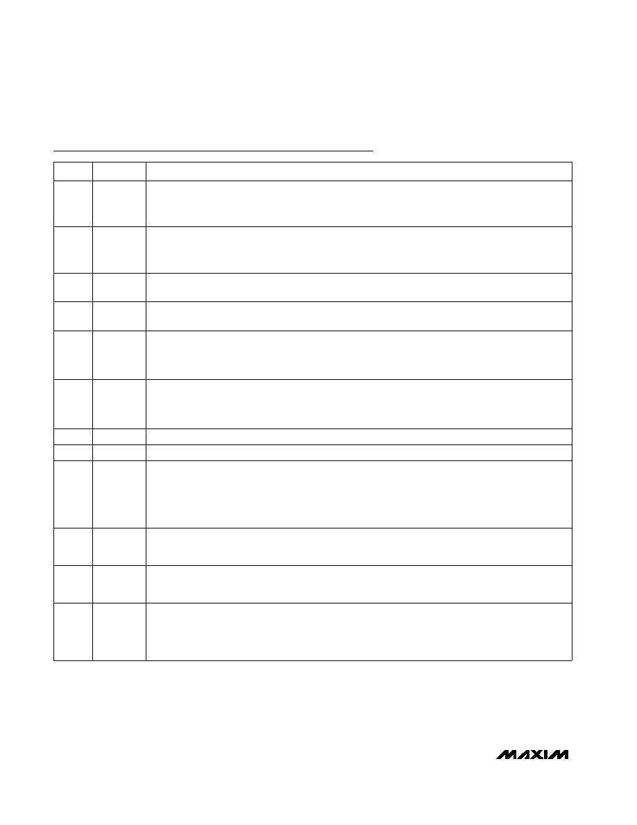
Pin Description (continued)
NAME
FUNCTION
PIN
17
CALGAIN-
Negative Gain Calibration Input. Used for system-gain calibration. It forms the negative input of a fully
differential input pair with CALGAIN+. Normally these inputs are connected to reference voltages in the
system. When system gain calibration is not required and the auto-sequence mode is used, the
CALGAIN+/CALGAIN- input pair provides an additional fully differential input channel.
18
CALGAIN+
Positive Gain Calibration Input. Used for system gain calibration. It forms the positive input of a fully differ-
ential input pair with CALGAIN-. Normally these inputs are connected to reference voltages in the system.
When system gain calibration is not required and the auto-sequence mode is used, the CALGAIN+/
CALGAIN- input pair provides an additional fully differential input channel.
19
REFIN-
Negative Differential Reference Input. Bias REFIN- between V+ and AGND, provided that REFIN+ is more
positive than REFIN-.
20
REFIN+
Positive Differential Reference Input. Bias REFIN+ between V+ and AGND, provided that REFIN+ is more
positive than REFIN-.
21
CALOFF-
Negative Offset Calibration Input. Used for system offset calibration. It forms the negative input of a fully
differential input pair with CALOFF+. Normally these inputs are connected to zero-reference voltages in
the system. When system offset calibration is not required and the auto-sequence mode is used, the
CALOFF+/CALOFF- input pair provides an additional fully differential input channel.
22
CALOFF+
Positive Offset Calibration Input. Used for system offset calibration. It forms the positive input of a fully
differential input pair with CALOFF-. Normally these inputs are connected to zero-reference voltages in the
system. When system offset calibration is not required and the auto-sequence mode is used, the
CALOFF+/CALOFF- input pair provides an additional fully differential input channel.
23
DGND
Digital Ground. Reference point for digital circuitry.
24
VDD
Digital Supply Voltage (+2.7V to +5.25V)
25
INT
Interrupt Output. A logic low indicates that a new output word is available from the data register. INT
returns high upon completion of a full output word read operation. INT also returns high for short periods
(determined by the filter and clock control bits) if no data read has taken place. A logic high indicates
internal activity, and a read operation should not be attempted under this condition. INT can also provide
a strobe to indicate valid data at DOUT (MDOUT = 1).
26
DOUT
Serial Data Output. DOUT outputs data from the internal shift register containing information from the
Communications Register, Global Setup Registers, Transfer Function Registers, or Data Register. DOUT
can also provide the digital bit stream directly from the
Σ- modulator (MDOUT = 1).
27
DIN
Serial Data Input. Data on DIN is written to the input shift register and later transferred to the
Communications Register, Global Setup Registers, Special Function Register, or Transfer Function
Registers, depending on the register selection bits in the Communications Register.
28
SCLK
Serial Clock Input. Apply an external serial clock to transfer data to and from the MAX1400. This serial
clock can be continuous, with data transmitted in a train of pulses, or intermittent. If CS is used to frame
the data transfer, then SCLK can idle high or low between conversions and CS determines the desired
active clock edge (see the Selecting Clock Polarity section). If CS is tied permanently low, SCLK must idle
high between data transfers.
相关PDF资料 |
PDF描述 |
|---|---|
| UP050SL130J-KEC | CAP CER 13PF 50V 5% AXIAL |
| UP050SL130J-B-B | CAP CER 13PF 50V 5% AXIAL |
| MAX172BCWG+ | IC ADC 12BIT CMOS 24-SOIC |
| VE-B43-MX-F1 | CONVERTER MOD DC/DC 24V 75W |
| VE-20J-MX | CONVERTER MOD DC/DC 36V 75W |
相关代理商/技术参数 |
参数描述 |
|---|---|
| MAX1400EAI+ | 功能描述:模数转换器 - ADC 18-Bit 5Ch 4.8ksps 2.5V Precision ADC RoHS:否 制造商:Texas Instruments 通道数量:2 结构:Sigma-Delta 转换速率:125 SPs to 8 KSPs 分辨率:24 bit 输入类型:Differential 信噪比:107 dB 接口类型:SPI 工作电源电压:1.7 V to 3.6 V, 2.7 V to 5.25 V 最大工作温度:+ 85 C 安装风格:SMD/SMT 封装 / 箱体:VQFN-32 |
| MAX1400EAI+T | 功能描述:模数转换器 - ADC 18-Bit 5Ch 4.8ksps 2.5V Precision ADC RoHS:否 制造商:Texas Instruments 通道数量:2 结构:Sigma-Delta 转换速率:125 SPs to 8 KSPs 分辨率:24 bit 输入类型:Differential 信噪比:107 dB 接口类型:SPI 工作电源电压:1.7 V to 3.6 V, 2.7 V to 5.25 V 最大工作温度:+ 85 C 安装风格:SMD/SMT 封装 / 箱体:VQFN-32 |
| MAX1400EAI-T | 功能描述:模数转换器 - ADC RoHS:否 制造商:Texas Instruments 通道数量:2 结构:Sigma-Delta 转换速率:125 SPs to 8 KSPs 分辨率:24 bit 输入类型:Differential 信噪比:107 dB 接口类型:SPI 工作电源电压:1.7 V to 3.6 V, 2.7 V to 5.25 V 最大工作温度:+ 85 C 安装风格:SMD/SMT 封装 / 箱体:VQFN-32 |
| MAX1400EVKIT | 制造商:Maxim Integrated Products 功能描述:MAX1402 EVALUATION KIT/EVALUATION SYSTEM - Boxed Product (Development Kits) |
| MAX1401CAI | 功能描述:模数转换器 - ADC RoHS:否 制造商:Texas Instruments 通道数量:2 结构:Sigma-Delta 转换速率:125 SPs to 8 KSPs 分辨率:24 bit 输入类型:Differential 信噪比:107 dB 接口类型:SPI 工作电源电压:1.7 V to 3.6 V, 2.7 V to 5.25 V 最大工作温度:+ 85 C 安装风格:SMD/SMT 封装 / 箱体:VQFN-32 |
发布紧急采购,3分钟左右您将得到回复。