- 您现在的位置:买卖IC网 > PDF目录17008 > MAX1403EVKIT (Maxim Integrated Products)EVAL KIT FOR MAX1403 PDF资料下载
参数资料
| 型号: | MAX1403EVKIT |
| 厂商: | Maxim Integrated Products |
| 文件页数: | 3/36页 |
| 文件大小: | 0K |
| 描述: | EVAL KIT FOR MAX1403 |
| 产品培训模块: | Lead (SnPb) Finish for COTS Obsolescence Mitigation Program |
| 标准包装: | 1 |
| ADC 的数量: | 1 |
| 位数: | 18 |
| 采样率(每秒): | 480 |
| 数据接口: | 串行 |
| 输入范围: | ±VREF/增益 |
| 在以下条件下的电源(标准): | 16.9mW @ 480SPS |
| 工作温度: | 0°C ~ 70°C |
| 已用 IC / 零件: | MAX1403 |
| 已供物品: | 板,CD |
第1页第2页当前第3页第4页第5页第6页第7页第8页第9页第10页第11页第12页第13页第14页第15页第16页第17页第18页第19页第20页第21页第22页第23页第24页第25页第26页第27页第28页第29页第30页第31页第32页第33页第34页第35页第36页
MAX1403
+3V, 18-Bit, Low-Power, Multichannel,
Oversampling (Sigma-Delta) ADC
______________________________________________________________________________________
11
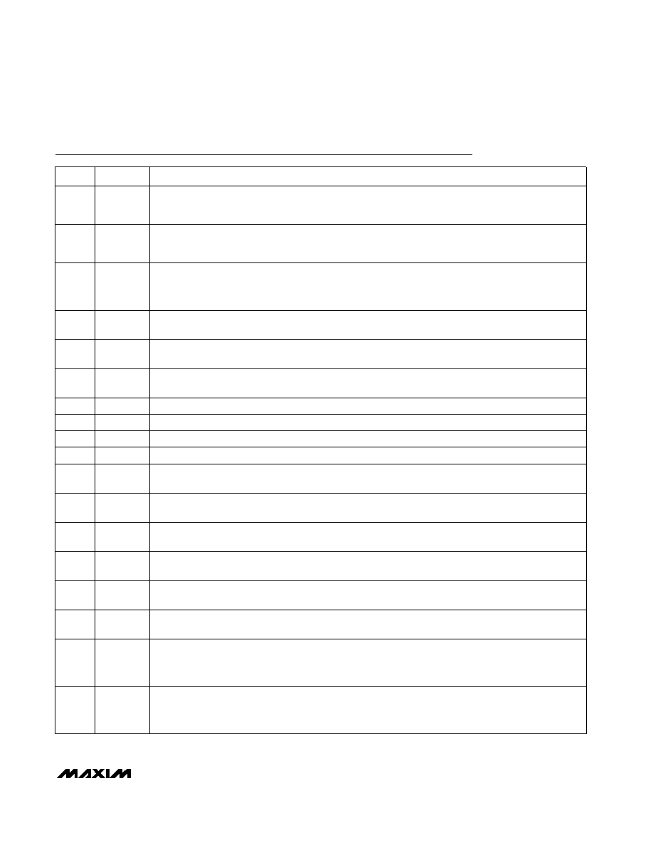
Pin Description
15
AIN5
Analog Input Channel 5. Used as a differential or pseudo-differential input with AIN6 (see On-Chip
Registers section).
NAME
FUNCTION
1
CLKIN
Clock Input. A crystal can be connected across CLKIN and CLKOUT. Alternatively, drive CLKIN with a
CMOS-compatible clock at a nominal frequency of 2.4576MHz or 1.024MHz, and leave CLKOUT uncon-
nected. Frequencies of 4.9152MHz and 2.048MHz may be used if the X2CLK control bit is set to 1.
PIN
2
CLKOUT
Clock Output. When deriving the master clock from a crystal, connect the crystal between CLKIN and
CLKOUT. In this mode, the on-chip clock signal is not available at CLKOUT. Leave CLKOUT unconnected
when CLKIN is driven with an external clock.
3
CS
Chip-Select Input. This active-low logic input is used to enable the digital interface. With CS hard-wired
low, the MAX1403 operates in its 3-wire interface mode with SCLK, DIN, and DOUT used to interface to
the device. CS is used either to select the device in systems with more than one device on the serial bus,
or as a frame-synchronization signal for the MAX1403, when a continuous SCLK is used.
4
RESET
Active-Low Reset Input. Drive low to reset the control logic, interface logic, digital filter, and analog modu-
lator to power-on status. RESET must be high and CLKIN must be toggling in order to exit reset.
5
DS1
Digital Input for Auxiliary Data Input Bit 1. The status of this bit is reflected in the output data by bit D4.
Used to communicate the status of DS1 via the serial interface.
6
DS0
Digital Input for Auxiliary Data Input Bit 0. The status of this bit is reflected in the output data by bit D3.
Used to communicate the status of DS0 via the serial interface.
7
OUT2
Transducer Excitation Current Source 2
8
OUT1
Transducer Excitation Current Source 1
9
AGND
Analog Ground. Reference point for the analog circuitry. AGND connects to the IC substrate.
10
V+
Analog Positive Supply Voltage (+2.7V to +3.6V).
11
AIN1
Analog Input Channel 1. May be used as a pseudo-differential input with AIN6 as common, or as the posi-
tive input of the AIN1/AIN2 differential analog input pair (see On-Chip Registers section).
12
AIN2
Analog Input Channel 2. May be used as a pseudo-differential input with AIN6 as common, or as the neg-
ative input of the AIN1/AIN2 differential analog input pair (see On-Chip Registers section).
13
AIN3
Analog Input Channel 3. May be used as a pseudo-differential input with AIN6 as common, or as the posi-
tive input of the AIN3/AIN4 differential analog input pair (see On-Chip Registers section).
14
AIN4
Analog Input Channel 4. May be used as a pseudo-differential input with AIN6 as common, or as the neg-
ative input of the AIN3/AIN4 differential analog input pair (see On-Chip Registers section).
16
AIN6
Analog Input 6. May be used as a common point for AIN1 through AIN5 in pseudo-differential mode, or as
the negative input of the AIN5/AIN6 differential analog input pair (see On-Chip Registers section).
17
CALGAIN-
Negative Gain Calibration Input. Used for system gain calibration. It forms the negative input of a fully
differential input pair with CALGAIN+. Normally these inputs are connected to reference voltages in the
system. When system gain calibration is not required and the auto-sequence mode is used, the
CALGAIN+/CALGAIN- input pair provides an additional fully differential input channel.
18
CALGAIN+
Positive Gain Calibration Input. Used for system gain calibration. It forms the positive input of a fully
differential input pair with CALGAIN-. Normally these inputs are connected to reference voltages in the
system. When system gain calibration is not required and the auto-sequence mode is used, the
CALGAIN+/CALGAIN- input pair provides an additional fully differential input channel.
相关PDF资料 |
PDF描述 |
|---|---|
| GEC36DRES-S13 | CONN EDGECARD 72POS .100 EXTEND |
| VI-2W4-EY | CONVERTER MOD DC/DC 48V 50W |
| 380LX121M400J022 | CAP ALUM 120UF 400V 20% SNAP |
| SDR7045-470K | INDUCTOR POWER 47UH 10% SMD |
| AC1059 | SOCKET FOR MODEL AD210 IC |
相关代理商/技术参数 |
参数描述 |
|---|---|
| MAX1403EVL11 | 功能描述:数据转换 IC 开发工具 MAX1403 Eval Kit RoHS:否 制造商:Texas Instruments 产品:Demonstration Kits 类型:ADC 工具用于评估:ADS130E08 接口类型:SPI 工作电源电压:- 6 V to + 6 V |
| MAX1403EVSYSTEM | 制造商:Maxim Integrated Products 功能描述:EVALUATION SYSTEM FOR THE MAX1403 - Boxed Product (Development Kits) |
| MAX1406C/D | 功能描述:RS-232接口集成电路 RoHS:否 制造商:Exar 数据速率:52 Mbps 工作电源电压:5 V 电源电流:300 mA 工作温度范围:- 40 C to + 85 C 安装风格:SMD/SMT 封装 / 箱体:LQFP-100 封装: |
| MAX1406CAE | 功能描述:RS-232接口集成电路 RoHS:否 制造商:Exar 数据速率:52 Mbps 工作电源电压:5 V 电源电流:300 mA 工作温度范围:- 40 C to + 85 C 安装风格:SMD/SMT 封装 / 箱体:LQFP-100 封装: |
| MAX1406CAE+ | 功能描述:RS-232接口集成电路 15kV ESD-Protected 230kbps RS-232 LD/Rc RoHS:否 制造商:Exar 数据速率:52 Mbps 工作电源电压:5 V 电源电流:300 mA 工作温度范围:- 40 C to + 85 C 安装风格:SMD/SMT 封装 / 箱体:LQFP-100 封装: |
发布紧急采购,3分钟左右您将得到回复。