- 您现在的位置:买卖IC网 > PDF目录2008 > MAX1415AEWE+T (Maxim Integrated Products)IC ADC 16BIT DELTA SIGMA 16-SOIC PDF资料下载
参数资料
| 型号: | MAX1415AEWE+T |
| 厂商: | Maxim Integrated Products |
| 文件页数: | 17/36页 |
| 文件大小: | 0K |
| 描述: | IC ADC 16BIT DELTA SIGMA 16-SOIC |
| 产品培训模块: | Lead (SnPb) Finish for COTS Obsolescence Mitigation Program |
| 标准包装: | 1,000 |
| 位数: | 16 |
| 采样率(每秒): | 500 |
| 数据接口: | MICROWIRE?,QSPI?,串行,SPI? |
| 转换器数目: | 1 |
| 功率耗散(最大): | 762mW |
| 电压电源: | 单电源 |
| 工作温度: | -45°C ~ 85°C |
| 安装类型: | 表面贴装 |
| 封装/外壳: | 16-SOIC(0.295",7.50mm 宽) |
| 供应商设备封装: | 16-SOIC W |
| 包装: | 带卷 (TR) |
| 输入数目和类型: | 2 个差分,单极;2 个差分,双极 |
第1页第2页第3页第4页第5页第6页第7页第8页第9页第10页第11页第12页第13页第14页第15页第16页当前第17页第18页第19页第20页第21页第22页第23页第24页第25页第26页第27页第28页第29页第30页第31页第32页第33页第34页第35页第36页
MAX1415/MAX1416
The default state of the MAX1415/MAX1416 is to wait
for a write to the communications register. Any write or
read operation on the MAX1415/MAX1416 is a two-step
process. First, a command byte is written to the com-
munications register. This command selects the input
channel, the desired register for the next read or write
operation, and whether the next operation is a read or a
write. The second step is to read from or write to the
selected register. At the end of the data-transfer cycle,
the device returns to the default state. See the
Performing a Conversion section for examples.
If the serial communication is lost, write 32 ones to the ser-
ial interface to return the MAX1415/MAX1416 to the default
state. The registers are not reset after this operation.
Communications Register
The byte-wide communications register is bidirectional
so it can be written and read. The byte written to the
communications register indicates the next read or write
operation on the selected register, the power-down
mode, and the analog input channel (see Table 6). The
DRDY bit indicates the conversion status.
0/
DRDY: (Default = 0) Communication-Start/Data-Ready
Bit. Write a 0 to the 0/
DRDY bit to start a write operation to
the communications register. If 0/
DRDY = 1, then the
device waits until a 0 is written to 0/
DRDY before continu-
ing to load the remaining bits. For a read operation, the
0/
DRDY bit shows the status of the conversion. The
DRDY bit returns a 0 if the conversion is complete and
the data is ready.
DRDY returns a 1 if the new data has
been read and the next conversion is not yet complete. It
has the same value as the
DRDY output pin.
RS2, RS1, RS0: (Default = 0, 0, 0) Register-Select Bits.
RS2, RS1, and RS0 select the next register to be
accessed as shown in Table 7.
R/
W: (Default = 0) Read-/Write-Select Bit. Use this bit to
select if the next register access is a read or a write
operation. Set R/
W = 0 to select a write operation, or set
R/
W = 1 for a read operation on the selected register.
PD: (Default = 0) Power-Down Control Bit. Set PD = 1
to initiate power-down mode. Set PD = 0 to take the
device out of power-down mode. If the internal oscilla-
tor or external crystal/resonator is used and CLKDIS =
0, CLKOUT remains active during power-down mode to
provide a clock source for other devices in the system.
CH1, CH0: (Default = 0, 0) Channel-Select Bit. Write to
the CH1 and CH0 bits to select the conversion channel or
to access the calibration data shown in Table 8. The cali-
bration coefficients of a particular channel are stored in
one of the three offset and gain register pairs in Table 8.
Set CH1 = 1 and CH0 = 0 to evaluate the noise perfor-
mance of the part without external noise sources. In this
noise-evaluation mode, connect AIN1- to an external volt-
age within the allowable common-mode range.
Setup Register
The byte-wide setup register is bidirectional so it can
be written and read. The byte written to the setup regis-
ter sets the calibration modes, PGA gain, unipolar/bipo-
lar mode, buffer enable, and conversion start (see
Table 9).
MD1, MD0: (Default = 0, 0) Mode-Select Bits. See
Table 10 for normal operating mode, self-calibration,
zero-scale calibration, or full-scale calibration-mode
selection.
16-Bit, Low-Power, 2-Channel,
Sigma-Delta ADCs
24
______________________________________________________________________________________
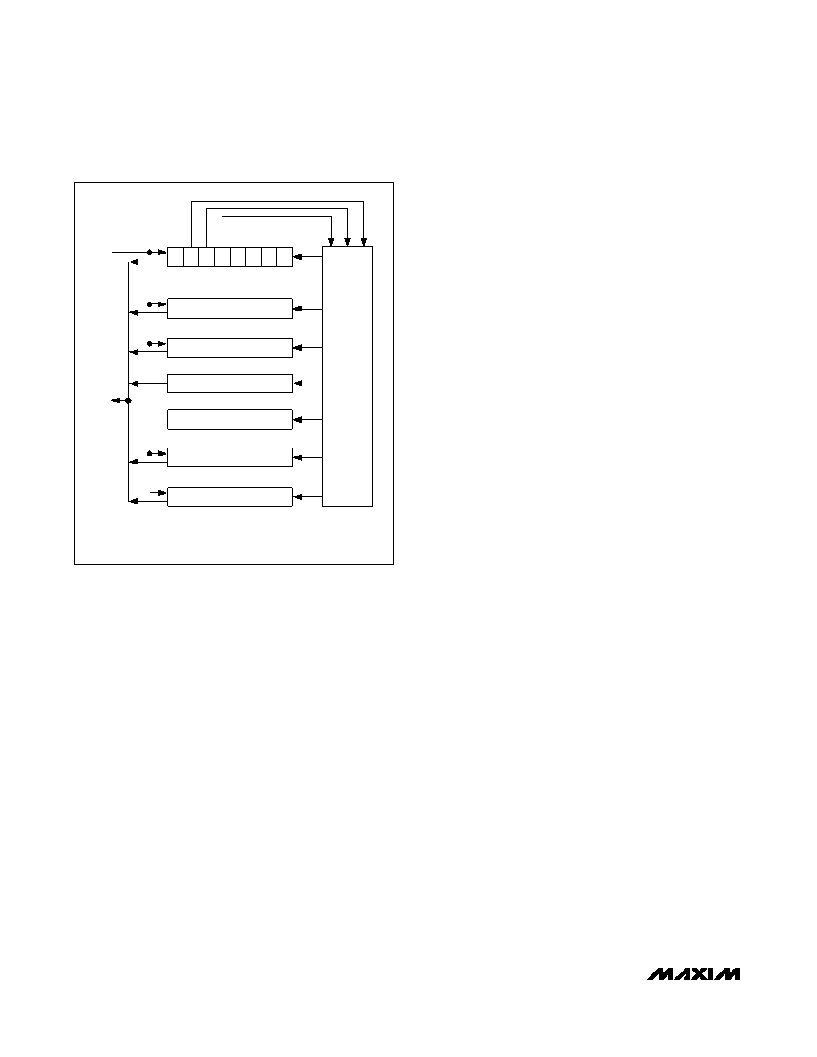
SETUP REGISTER (8 BITS)
RS2 RS1 RS0
CLOCK REGISTER (8 BITS)
DATA REGISTER (16 BITS)
TEST REGISTER (8 BITS)*
OFFSET REGISTER (24 BITS)
GAIN REGISTER (24 BITS)
COMMUNICATIONS REGISTER
REGISTER
SELECT
DECODER
DIN
DOUT
*THE TEST REGISTER IS USED FOR FACTORY TESTING ONLY.
Figure 10. Register Summary
相关PDF资料 |
PDF描述 |
|---|---|
| MAX1421CCM+D | IC ADC 12BIT 40MSPS 48LQFP |
| MAX1426EAI+T | IC ADC 10BITS 10MSPS 28SSOP |
| MAX1434ECQ+D | IC ADC 10BIT 50MSPS 100-TQFP |
| MAX1444EHJ+T | IC ADC 10BIT 40MSPS 32-TQFP |
| MAX1499ECJ+ | IC ADC 3 1/2DIG W/LED DVR 32TQFP |
相关代理商/技术参数 |
参数描述 |
|---|---|
| MAX1415ENE | 制造商:Maxim Integrated Products 功能描述:16-BIT, LOW-POWER, 2-CHANNEL, SIGMA-DELTA ADC - Rail/Tube |
| MAX1415EPE | 功能描述:模数转换器 - ADC RoHS:否 制造商:Texas Instruments 通道数量:2 结构:Sigma-Delta 转换速率:125 SPs to 8 KSPs 分辨率:24 bit 输入类型:Differential 信噪比:107 dB 接口类型:SPI 工作电源电压:1.7 V to 3.6 V, 2.7 V to 5.25 V 最大工作温度:+ 85 C 安装风格:SMD/SMT 封装 / 箱体:VQFN-32 |
| MAX1415EPE+ | 功能描述:模数转换器 - ADC 16-Bit 2Ch .5ksps 1.75V Precision ADC RoHS:否 制造商:Texas Instruments 通道数量:2 结构:Sigma-Delta 转换速率:125 SPs to 8 KSPs 分辨率:24 bit 输入类型:Differential 信噪比:107 dB 接口类型:SPI 工作电源电压:1.7 V to 3.6 V, 2.7 V to 5.25 V 最大工作温度:+ 85 C 安装风格:SMD/SMT 封装 / 箱体:VQFN-32 |
| MAX1415EUE | 功能描述:模数转换器 - ADC RoHS:否 制造商:Texas Instruments 通道数量:2 结构:Sigma-Delta 转换速率:125 SPs to 8 KSPs 分辨率:24 bit 输入类型:Differential 信噪比:107 dB 接口类型:SPI 工作电源电压:1.7 V to 3.6 V, 2.7 V to 5.25 V 最大工作温度:+ 85 C 安装风格:SMD/SMT 封装 / 箱体:VQFN-32 |
| MAX1415EUE+ | 功能描述:模数转换器 - ADC 16-Bit 2Ch .5ksps 1.75V Precision ADC RoHS:否 制造商:Texas Instruments 通道数量:2 结构:Sigma-Delta 转换速率:125 SPs to 8 KSPs 分辨率:24 bit 输入类型:Differential 信噪比:107 dB 接口类型:SPI 工作电源电压:1.7 V to 3.6 V, 2.7 V to 5.25 V 最大工作温度:+ 85 C 安装风格:SMD/SMT 封装 / 箱体:VQFN-32 |
发布紧急采购,3分钟左右您将得到回复。