- 您现在的位置:买卖IC网 > PDF目录1936 > MAX1464AAI+T (Maxim Integrated Products)IC SENSOR SIGNAL COND 28-SSOP PDF资料下载
参数资料
| 型号: | MAX1464AAI+T |
| 厂商: | Maxim Integrated Products |
| 文件页数: | 5/47页 |
| 文件大小: | 0K |
| 描述: | IC SENSOR SIGNAL COND 28-SSOP |
| 产品培训模块: | Lead (SnPb) Finish for COTS Obsolescence Mitigation Program |
| 标准包装: | 2,000 |
| 类型: | 信号调节器 |
| 输入类型: | 模拟 |
| 输出类型: | 逻辑 |
| 接口: | SPI |
| 电流 - 电源: | 890µA |
| 安装类型: | 表面贴装 |
| 封装/外壳: | 28-SSOP(0.209",5.30mm 宽) |
| 供应商设备封装: | 28-SSOP |
| 包装: | 带卷 (TR) |
第1页第2页第3页第4页当前第5页第6页第7页第8页第9页第10页第11页第12页第13页第14页第15页第16页第17页第18页第19页第20页第21页第22页第23页第24页第25页第26页第27页第28页第29页第30页第31页第32页第33页第34页第35页第36页第37页第38页第39页第40页第41页第42页第43页第44页第45页第46页第47页
MAX1464
Low-Power, Low-Noise Multichannel
Sensor Signal Processor
13
Maxim Integrated
On-Chip Temperature Sensing
The on-chip temperature sensor changes +2mV/°C over
the operating range. The ADC converts the temperature
sensor in a similar manner as the sensor inputs. During
an ADC conversion of the temperature sensor, the ADC
automatically uses four times the internal 1.25V reference
as the ADC full-scale reference (5V). The temperature
data format is 15-bit plus sign in two’s-complement for-
mat. Gain offset compensation can be programmed to
utilize the full-scale range of the ADC. Offset compensa-
tion by the CO DAC is provided so that the nominal tem-
perature measurement can be centered at the ADC
output value. Use the CPU to provide additional digital
gain and offset correction.
Output Format
There are two output modules in the MAX1464—DOP1
(DAC Op Amp PWM 1) and DOP2 (DAC Op Amp PWM
2). Each of the DOP modules contains a 16-bit DAC, a
12-bit digital PWM converter, a small op amp, and a
large op amp with high-output-drive capability. Each
module can be configured in several different modes to
suit a wide range of output signal requirements. Either
the DAC or the PWM can be selected as the primary
output signal. The DAC output signal must be routed to
one of the two op amps before being made available to
a device pin. See the
DAC, Op Amp, PWM Modules
(DPOn) section for details. Additional digital outputs are
available on the GPIOs.
Initialization
A user-defined initialization routine is required to config-
ure the oscillator frequency and various analog modules,
e.g., PGA gain, ADC resolution, ADC clock settings, etc.
After the initialization routine, the CPU can start execution
of the main program.
Power-On Reset (POR)
The MAX1464 contains a POR circuit to disable CPU
execution until adequate VDD and VDDF voltage are
available for operation. Once the power-on state has
been reached, the MAX1464 is kept under reset condi-
tion for 250s before the CPU starts execution. Below
the POR threshold, all internal CPU registers are set to
their POR default state. Power-on control bits for internal
modules are reset to the OFF condition.
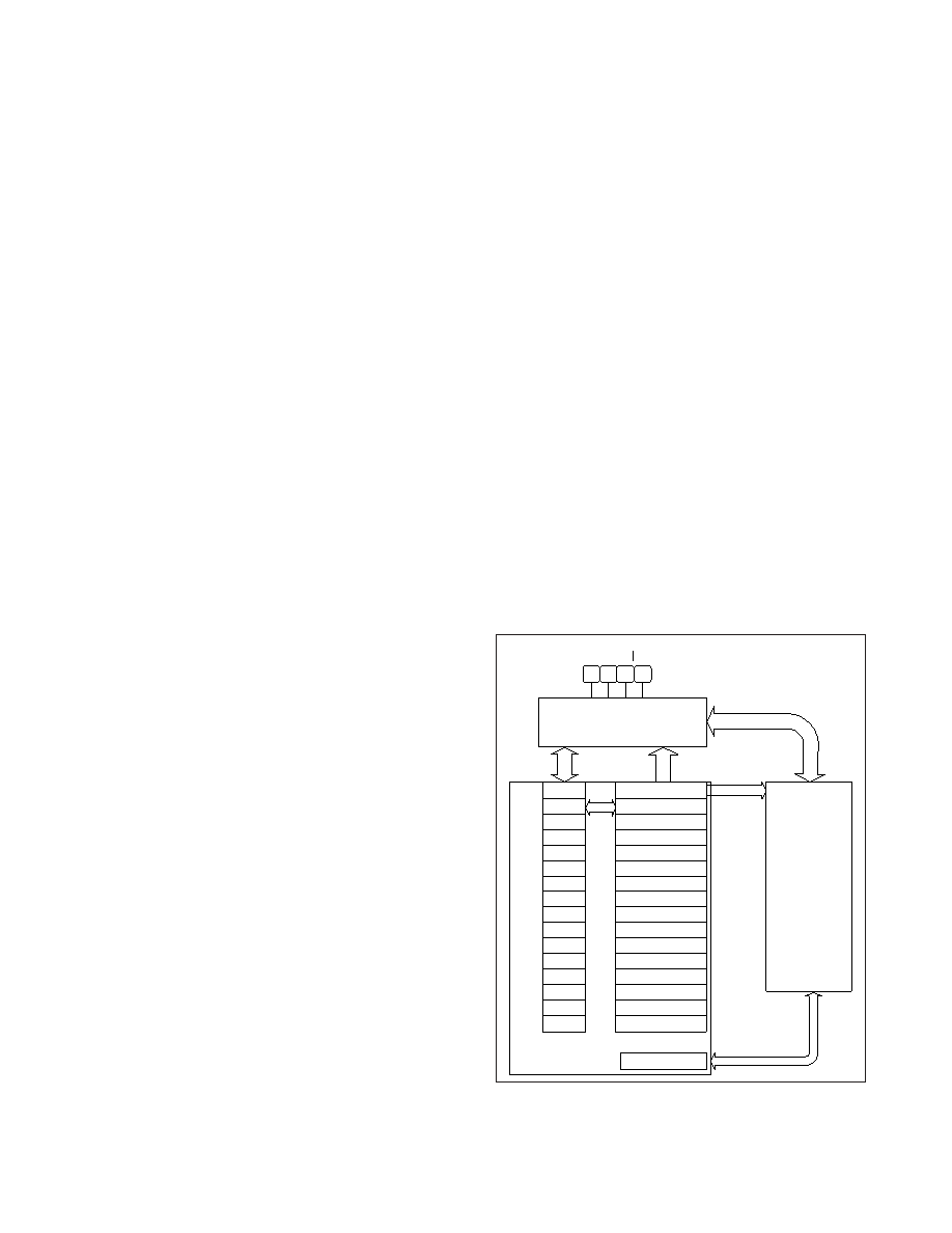
CPU Architecture
The CPU provides a wide range of functionality to be
incorporated in an embedded system. The CPU can
compensate nonlinear and temperature-dependent sen-
sors, check for over/underlimit conditions, output sensor
or temperature data as an analog signal or pulse-width-
modulated digital signal, and execute control strategies.
The CPU can perform a limited amount of signal pro-
cessing (filtering). A timer is included so that uniform
sampling (equally spaced ADC conversions) of the
input sensors can be performed.
The CPU registers and ports are implemented in volatile,
static memory. There are several registers contained in
various peripheral modules that provide module configu-
ration settings, control functions, and data. These module
registers are accessible through an indirect addressing
scheme as described in detail in the
CPU Registers,
CPU Ports, and Modules sections. Figure 3 shows the
CPU architecture.
CPU Registers
The MAX1464 incorporates a CPU with 16 internal regis-
ters. All the CPU registers have a 16-bit data word width.
Five of the 16 registers have predefined functional oper-
ations that are dependent on the instruction being exe-
cuted. The remaining registers are general purpose.
The CPU registers are embedded in the CPU itself and
are not all directly accessible by the serial interface. The
accumulator register (A), the pointer register (P), and the
instruction (FLASH data) can be read through the serial
interface when the CPU is halted. This enables a single-
FLASH MEMORY
(4kB)
SERIAL INTERFACE
SCLK
DI
DO
CS
R0
POINTER (P)
R1 ACCUMULATOR (A)
R2
R3 MULTIPLICAND (N)
R4 MULTIPLIER (M)
R6
R7
R8
R9
RA
RB
RC
RD
RE
RF
P0
P1
P2
P1
P3
P4
P5
P6
P7
P8
PA
PB
PC
PD
PE
PF
CPU REGISTERS
INSTRUCTION
CPU
FLASH DATA
ADDRESS
CPU PORTS
R5
INDEX (I)
Figure 3. CPU Architecture
相关PDF资料 |
PDF描述 |
|---|---|
| MAX1474AXT+T | IC ELECTRONIC CAPACITOR SC70-6 |
| MAX14753EUE+T | IC MULTIPLEXER DUAL 4X1 16TSSOP |
| MAX14756EUE+T | IC ANLG SWITCH SPST QUAD 16TSSOP |
| MAX14759ETA+ | IC SWITCH ANALOG 8-TDFN-EP |
| MAX14764ETA+T | IC ANALOG SWITCH |
相关代理商/技术参数 |
参数描述 |
|---|---|
| MAX1464CAI | 功能描述:数字信号处理器和控制器 - DSP, DSC RoHS:否 制造商:Microchip Technology 核心:dsPIC 数据总线宽度:16 bit 程序存储器大小:16 KB 数据 RAM 大小:2 KB 最大时钟频率:40 MHz 可编程输入/输出端数量:35 定时器数量:3 设备每秒兆指令数:50 MIPs 工作电源电压:3.3 V 最大工作温度:+ 85 C 封装 / 箱体:TQFP-44 安装风格:SMD/SMT |
| MAX1464CAI+ | 功能描述:数字信号处理器和控制器 - DSP, DSC Low-Power Low-Noise Multichannel Sensor Signal Processor RoHS:否 制造商:Microchip Technology 核心:dsPIC 数据总线宽度:16 bit 程序存储器大小:16 KB 数据 RAM 大小:2 KB 最大时钟频率:40 MHz 可编程输入/输出端数量:35 定时器数量:3 设备每秒兆指令数:50 MIPs 工作电源电压:3.3 V 最大工作温度:+ 85 C 封装 / 箱体:TQFP-44 安装风格:SMD/SMT |
| MAX1464CAI+T | 功能描述:数字信号处理器和控制器 - DSP, DSC Low-Power Low-Noise Multichannel Sensor Signal Processor RoHS:否 制造商:Microchip Technology 核心:dsPIC 数据总线宽度:16 bit 程序存储器大小:16 KB 数据 RAM 大小:2 KB 最大时钟频率:40 MHz 可编程输入/输出端数量:35 定时器数量:3 设备每秒兆指令数:50 MIPs 工作电源电压:3.3 V 最大工作温度:+ 85 C 封装 / 箱体:TQFP-44 安装风格:SMD/SMT |
| MAX1464CAI-T | 功能描述:数字信号处理器和控制器 - DSP, DSC RoHS:否 制造商:Microchip Technology 核心:dsPIC 数据总线宽度:16 bit 程序存储器大小:16 KB 数据 RAM 大小:2 KB 最大时钟频率:40 MHz 可编程输入/输出端数量:35 定时器数量:3 设备每秒兆指令数:50 MIPs 工作电源电压:3.3 V 最大工作温度:+ 85 C 封装 / 箱体:TQFP-44 安装风格:SMD/SMT |
| MAX1464EAI | 功能描述:数字信号处理器和控制器 - DSP, DSC RoHS:否 制造商:Microchip Technology 核心:dsPIC 数据总线宽度:16 bit 程序存储器大小:16 KB 数据 RAM 大小:2 KB 最大时钟频率:40 MHz 可编程输入/输出端数量:35 定时器数量:3 设备每秒兆指令数:50 MIPs 工作电源电压:3.3 V 最大工作温度:+ 85 C 封装 / 箱体:TQFP-44 安装风格:SMD/SMT |
发布紧急采购,3分钟左右您将得到回复。