- 您现在的位置:买卖IC网 > PDF目录224187 > MAX147AEAP+ (MAXIM INTEGRATED PRODUCTS INC) +2.7V, Low-Power, 8-Channel, Serial 12-Bit ADCs PDF资料下载
参数资料
| 型号: | MAX147AEAP+ |
| 厂商: | MAXIM INTEGRATED PRODUCTS INC |
| 元件分类: | ADC |
| 英文描述: | +2.7V, Low-Power, 8-Channel, Serial 12-Bit ADCs |
| 中文描述: | 8-CH 12-BIT SUCCESSIVE APPROXIMATION ADC, SERIAL ACCESS, PDSO20 |
| 封装: | SSOP-20 |
| 文件页数: | 13/28页 |
| 文件大小: | 746K |
| 代理商: | MAX147AEAP+ |
第1页第2页第3页第4页第5页第6页第7页第8页第9页第10页第11页第12页当前第13页第14页第15页第16页第17页第18页第19页第20页第21页第22页第23页第24页第25页第26页第27页第28页
MAX146/MAX147
+2.7V, Low-Power, 8-Channel,
Serial 12-Bit ADCs
20
______________________________________________________________________________________
VREF, the DC input resistance is a minimum of 18k
.
During conversion, an external reference at VREF must
deliver up to 350A DC load current and have 10
or
less output impedance. If the reference has a higher
output impedance or is noisy, bypass it close to the
VREF pin with a 4.7F capacitor.
Using the REFADJ input makes buffering the external
reference unnecessary. To use the direct VREF input,
disable the internal buffer by tying REFADJ to VDD. In
power-down, the input bias current to REFADJ is typi-
cally 25A (MAX146) with REFADJ tied to VDD. Pull
REFADJ to AGND to minimize the input bias current in
power-down.
Transfer Function
Table 7 shows the full-scale voltage ranges for unipolar
and bipolar modes.
The external reference must have a temperature coeffi-
cient of 4ppm/°C or less to achieve accuracy to within
1LSB over the 0°C to +70°C commercial temperature
range.
Figure 17 depicts the nominal, unipolar input/output
(I/O) transfer function, and Figure 18 shows the bipolar
input/output transfer function. Code transitions occur
halfway between successive-integer LSB values.
Output coding is binary, with 1LSB = 610V (2.500V /
4096) for unipolar operation, and 1LSB = 610V
[(2.500V / 2 - -2.500V / 2) / 4096] for bipolar operation.
Layout, Grounding, and Bypassing
For best performance, use printed circuit boards.
Wire-wrap boards are not recommended. Board layout
should ensure that digital and analog signal lines are
separated from each other. Do not run analog and digi-
tal (especially clock) lines parallel to one another, or
digital lines underneath the ADC package.
Figure 19 shows the recommended system ground
connections. Establish a single-point analog ground
(star ground point) at AGND, separate from the logic
ground. Connect all other analog grounds and DGND
to the star ground. No other digital system ground
should be connected to this ground. For lowest-noise
operation, the ground return to the star ground’s power
supply should be low impedance and as short as
possible.
High-frequency noise in the VDD power supply may
affect the high-speed comparator in the ADC. Bypass
the supply to the star ground with 0.1F and 1F
capacitors close to pin 20 of the MAX146/MAX147.
Minimize capacitor lead lengths for best supply-noise
rejection. If the power supply is very noisy, a 10
resis-
tor can be connected as a lowpass filter (Figure 19).
High-Speed Digital Interfacing with QSPI
The MAX146/MAX147 can interface with QSPI using
the circuit in Figure 20 (fSCLK = 2.0MHz, CPOL = 0,
CPHA = 0). This QSPI circuit can be programmed to do a
conversion on each of the eight channels. The result is
stored in memory without taxing the CPU, since QSPI
incorporates its own microsequencer.
The MAX146/MAX147 are QSPI compatible up to the
maximum external clock frequency of 2MHz.
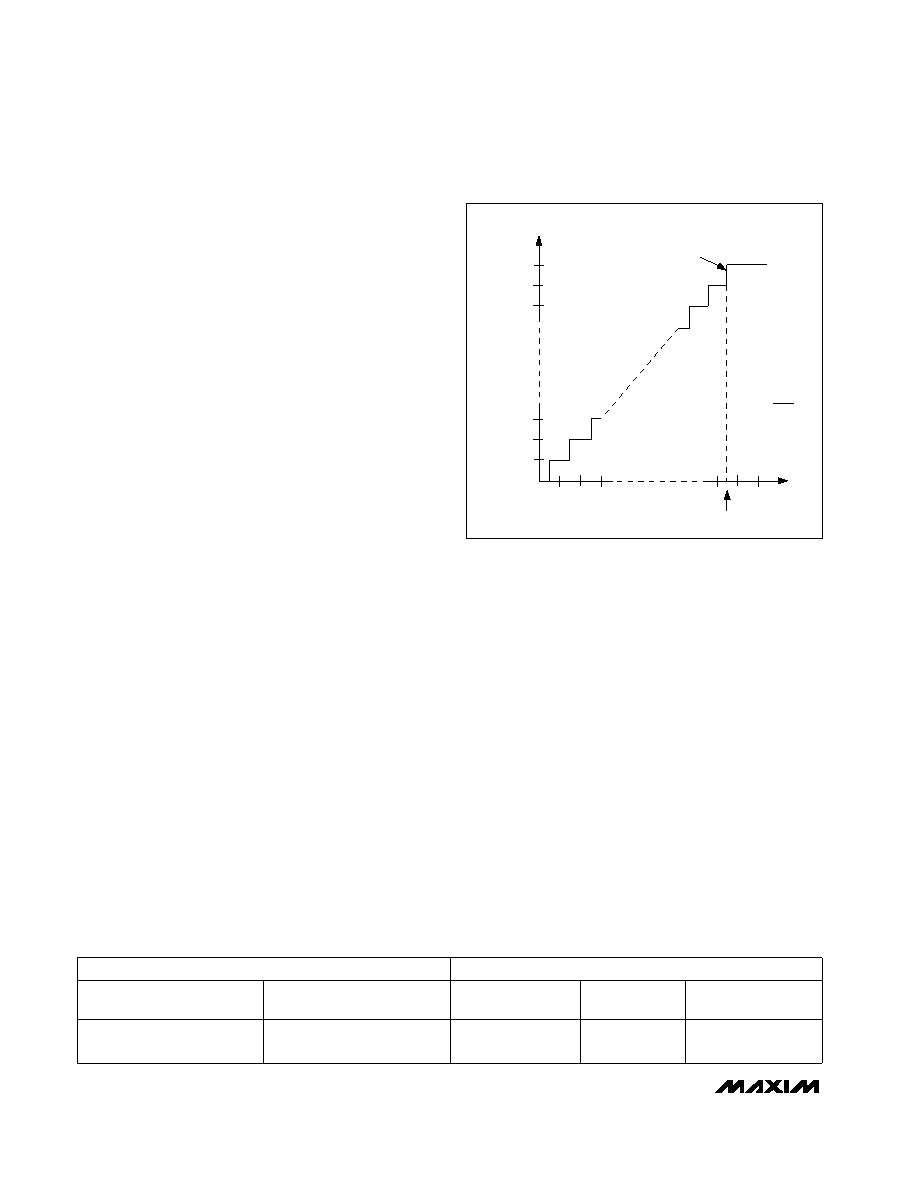
OUTPUT CODE
FULL-SCALE
TRANSITION
11 . . . 111
11 . . . 110
11 . . . 101
00 . . . 011
00 . . . 010
00 . . . 001
00 . . . 000
12
3
0
(COM)
FS
FS - 3/2LSB
FS = VREF + COM
ZS = COM
INPUT VOLTAGE (LSB)
1LSB =
VREF
4096
Figure 17. Unipolar Transfer Function, Full Scale (FS) = VREF
+ COM, Zero Scale (ZS) = COM
UNIPOLAR MODE
BIPOLAR MODE
Full Scale
Zero Scale
Positive
Zero
Negative
Full Scale
Scale
Full Scale
VREF + COM
COM
VREF / 2
COM
-VREF / 2
+ COM
Table 7. Full Scale and Zero Scale
相关PDF资料 |
PDF描述 |
|---|---|
| MAX147ACAP+T | +2.7V, Low-Power, 8-Channel, Serial 12-Bit ADCs |
| MAX147ACAP+ | +2.7V, Low-Power, 8-Channel, Serial 12-Bit ADCs |
| MAX146BEPP+ | +2.7V, Low-Power, 8-Channel, Serial 12-Bit ADCs |
| MAX146BEAP+ | +2.7V, Low-Power, 8-Channel, Serial 12-Bit ADCs |
| MAX146BEAP+T | +2.7V, Low-Power, 8-Channel, Serial 12-Bit ADCs |
相关代理商/技术参数 |
参数描述 |
|---|---|
| MAX147AEAP+ | 功能描述:模数转换器 - ADC 12-Bit 8Ch 133ksps 5.25V Precision ADC RoHS:否 制造商:Texas Instruments 通道数量:2 结构:Sigma-Delta 转换速率:125 SPs to 8 KSPs 分辨率:24 bit 输入类型:Differential 信噪比:107 dB 接口类型:SPI 工作电源电压:1.7 V to 3.6 V, 2.7 V to 5.25 V 最大工作温度:+ 85 C 安装风格:SMD/SMT 封装 / 箱体:VQFN-32 |
| MAX147AEAP+T | 功能描述:模数转换器 - ADC 12-Bit 8Ch 133ksps 5.25V Precision ADC RoHS:否 制造商:Texas Instruments 通道数量:2 结构:Sigma-Delta 转换速率:125 SPs to 8 KSPs 分辨率:24 bit 输入类型:Differential 信噪比:107 dB 接口类型:SPI 工作电源电压:1.7 V to 3.6 V, 2.7 V to 5.25 V 最大工作温度:+ 85 C 安装风格:SMD/SMT 封装 / 箱体:VQFN-32 |
| MAX147AEAP-T | 功能描述:模数转换器 - ADC RoHS:否 制造商:Texas Instruments 通道数量:2 结构:Sigma-Delta 转换速率:125 SPs to 8 KSPs 分辨率:24 bit 输入类型:Differential 信噪比:107 dB 接口类型:SPI 工作电源电压:1.7 V to 3.6 V, 2.7 V to 5.25 V 最大工作温度:+ 85 C 安装风格:SMD/SMT 封装 / 箱体:VQFN-32 |
| MAX147AEPP | 功能描述:模数转换器 - ADC RoHS:否 制造商:Texas Instruments 通道数量:2 结构:Sigma-Delta 转换速率:125 SPs to 8 KSPs 分辨率:24 bit 输入类型:Differential 信噪比:107 dB 接口类型:SPI 工作电源电压:1.7 V to 3.6 V, 2.7 V to 5.25 V 最大工作温度:+ 85 C 安装风格:SMD/SMT 封装 / 箱体:VQFN-32 |
| MAX147AEPP+ | 功能描述:模数转换器 - ADC 12-Bit 8Ch 133ksps 5.25V Precision ADC RoHS:否 制造商:Texas Instruments 通道数量:2 结构:Sigma-Delta 转换速率:125 SPs to 8 KSPs 分辨率:24 bit 输入类型:Differential 信噪比:107 dB 接口类型:SPI 工作电源电压:1.7 V to 3.6 V, 2.7 V to 5.25 V 最大工作温度:+ 85 C 安装风格:SMD/SMT 封装 / 箱体:VQFN-32 |
发布紧急采购,3分钟左右您将得到回复。