- 您现在的位置:买卖IC网 > PDF目录224187 > MAX147AEAP+ (MAXIM INTEGRATED PRODUCTS INC) +2.7V, Low-Power, 8-Channel, Serial 12-Bit ADCs PDF资料下载
参数资料
| 型号: | MAX147AEAP+ |
| 厂商: | MAXIM INTEGRATED PRODUCTS INC |
| 元件分类: | ADC |
| 英文描述: | +2.7V, Low-Power, 8-Channel, Serial 12-Bit ADCs |
| 中文描述: | 8-CH 12-BIT SUCCESSIVE APPROXIMATION ADC, SERIAL ACCESS, PDSO20 |
| 封装: | SSOP-20 |
| 文件页数: | 14/28页 |
| 文件大小: | 746K |
| 代理商: | MAX147AEAP+ |
第1页第2页第3页第4页第5页第6页第7页第8页第9页第10页第11页第12页第13页当前第14页第15页第16页第17页第18页第19页第20页第21页第22页第23页第24页第25页第26页第27页第28页
MAX146/MAX147
+2.7V, Low-Power, 8-Channel,
Serial 12-Bit ADCs
______________________________________________________________________________________
21
TMS320LC3x Interface
Figure 21 shows an application circuit to interface the
MAX146/MAX147 to the TMS320 in external clock mode.
The timing diagram for this interface circuit is shown in
Figure 22.
Use the following steps to initiate a conversion in the
MAX146/MAX147 and to read the results:
1) The TMS320 should be configured with CLKX
(transmit clock) as an active-high output clock and
CLKR (TMS320 receive clock) as an active-high
input clock. CLKX and CLKR on the TMS320 are
tied together with the MAX146/MAX147’s SCLK
input.
2) The MAX146/MAX147’s CS pin is driven low by the
TMS320’s XF_ I/O port to enable data to be clocked
into the MAX146/MAX147’s DIN.
3) An 8-bit word (1XXXXX11) should be written to the
MAX146/MAX147 to initiate a conversion and place
the device into external clock mode. Refer to Table
1 to select the proper XXXXX bit values for your
specific application.
4) The MAX146/MAX147’s SSTRB output is monitored
via the TMS320’s FSR input. A falling edge on the
SSTRB output indicates that the conversion is in
progress and data is ready to be received from the
MAX146/MAX147.
5) The TMS320 reads in one data bit on each of the
next 16 rising edges of SCLK. These data bits rep-
resent the 12-bit conversion result followed by four
trailing bits, which should be ignored.
6) Pull CS high to disable the MAX146/MAX147 until
the next conversion is initiated.
011 . . . 111
011 . . . 110
000 . . . 010
000 . . . 001
000 . . . 000
111 . . . 111
111 . . . 110
111 . . . 101
100 . . . 001
100 . . . 000
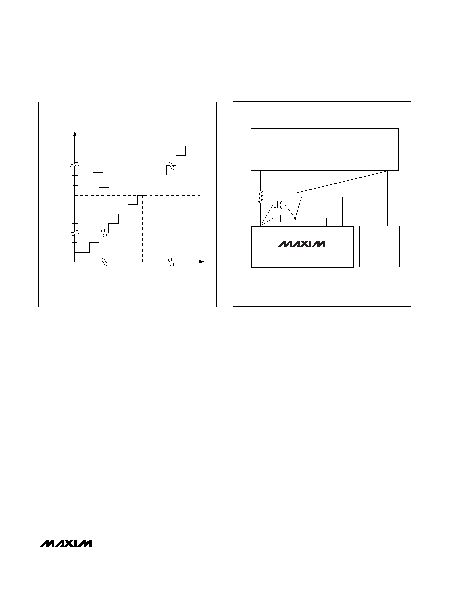
- FS
COM*
INPUT VOLTAGE (LSB)
OUTPUT CODE
ZS = COM
+FS - 1LSB
*COM
VREF / 2
+ COM
FS =
VREF
2
-FS =
+ COM
-VREF
2
1LSB =
VREF
4096
≤
Figure 18. Bipolar Transfer Function, Full Scale (FS) =
VREF / 2 + COM, Zero Scale (ZS) = COM
+3V
GND
SUPPLIES
DGND
+3V
DGND
COM
AGND
VDD
DIGITAL
CIRCUITRY
MAX146
MAX147
R* = 10
*OPTIONAL
Figure 19. Power-Supply Grounding Connection
相关PDF资料 |
PDF描述 |
|---|---|
| MAX147ACAP+T | +2.7V, Low-Power, 8-Channel, Serial 12-Bit ADCs |
| MAX147ACAP+ | +2.7V, Low-Power, 8-Channel, Serial 12-Bit ADCs |
| MAX146BEPP+ | +2.7V, Low-Power, 8-Channel, Serial 12-Bit ADCs |
| MAX146BEAP+ | +2.7V, Low-Power, 8-Channel, Serial 12-Bit ADCs |
| MAX146BEAP+T | +2.7V, Low-Power, 8-Channel, Serial 12-Bit ADCs |
相关代理商/技术参数 |
参数描述 |
|---|---|
| MAX147AEAP+ | 功能描述:模数转换器 - ADC 12-Bit 8Ch 133ksps 5.25V Precision ADC RoHS:否 制造商:Texas Instruments 通道数量:2 结构:Sigma-Delta 转换速率:125 SPs to 8 KSPs 分辨率:24 bit 输入类型:Differential 信噪比:107 dB 接口类型:SPI 工作电源电压:1.7 V to 3.6 V, 2.7 V to 5.25 V 最大工作温度:+ 85 C 安装风格:SMD/SMT 封装 / 箱体:VQFN-32 |
| MAX147AEAP+T | 功能描述:模数转换器 - ADC 12-Bit 8Ch 133ksps 5.25V Precision ADC RoHS:否 制造商:Texas Instruments 通道数量:2 结构:Sigma-Delta 转换速率:125 SPs to 8 KSPs 分辨率:24 bit 输入类型:Differential 信噪比:107 dB 接口类型:SPI 工作电源电压:1.7 V to 3.6 V, 2.7 V to 5.25 V 最大工作温度:+ 85 C 安装风格:SMD/SMT 封装 / 箱体:VQFN-32 |
| MAX147AEAP-T | 功能描述:模数转换器 - ADC RoHS:否 制造商:Texas Instruments 通道数量:2 结构:Sigma-Delta 转换速率:125 SPs to 8 KSPs 分辨率:24 bit 输入类型:Differential 信噪比:107 dB 接口类型:SPI 工作电源电压:1.7 V to 3.6 V, 2.7 V to 5.25 V 最大工作温度:+ 85 C 安装风格:SMD/SMT 封装 / 箱体:VQFN-32 |
| MAX147AEPP | 功能描述:模数转换器 - ADC RoHS:否 制造商:Texas Instruments 通道数量:2 结构:Sigma-Delta 转换速率:125 SPs to 8 KSPs 分辨率:24 bit 输入类型:Differential 信噪比:107 dB 接口类型:SPI 工作电源电压:1.7 V to 3.6 V, 2.7 V to 5.25 V 最大工作温度:+ 85 C 安装风格:SMD/SMT 封装 / 箱体:VQFN-32 |
| MAX147AEPP+ | 功能描述:模数转换器 - ADC 12-Bit 8Ch 133ksps 5.25V Precision ADC RoHS:否 制造商:Texas Instruments 通道数量:2 结构:Sigma-Delta 转换速率:125 SPs to 8 KSPs 分辨率:24 bit 输入类型:Differential 信噪比:107 dB 接口类型:SPI 工作电源电压:1.7 V to 3.6 V, 2.7 V to 5.25 V 最大工作温度:+ 85 C 安装风格:SMD/SMT 封装 / 箱体:VQFN-32 |
发布紧急采购,3分钟左右您将得到回复。