- 您现在的位置:买卖IC网 > PDF目录17275 > MAX15023EVKIT+ (Maxim Integrated Products)KIT EVALUATION FOR MAX15023 CTLR PDF资料下载
参数资料
| 型号: | MAX15023EVKIT+ |
| 厂商: | Maxim Integrated Products |
| 文件页数: | 9/28页 |
| 文件大小: | 0K |
| 描述: | KIT EVALUATION FOR MAX15023 CTLR |
| 产品培训模块: | Lead (SnPb) Finish for COTS Obsolescence Mitigation Program |
| 标准包装: | 1 |
| 主要目的: | DC/DC,步降 |
| 输出及类型: | 2,非隔离 |
| 输出电压: | 1.2V,3.3V |
| 电流 - 输出: | 10A,5A |
| 输入电压: | 9 ~ 16 V |
| 稳压器拓扑结构: | 降压 |
| 频率 - 开关: | 500kHz |
| 板类型: | 完全填充 |
| 已供物品: | 板 |
| 已用 IC / 零件: | MAX15023 |
第1页第2页第3页第4页第5页第6页第7页第8页当前第9页第10页第11页第12页第13页第14页第15页第16页第17页第18页第19页第20页第21页第22页第23页第24页第25页第26页第27页第28页
�� �
�
�MAX15023�
�Wide� 4.5V� to� 28V� Input,� Dual-Output�
�Synchronous� Buck� Controller�
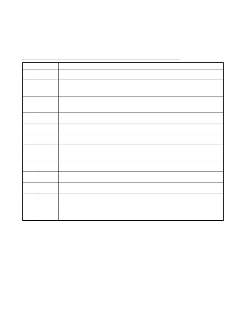
�Pin� Description�
�PIN�
�1�
�2�
�3�
�4�
�5�
�6�
�7�
�8�
�9�
�10�
�11�
�12�
�NAME�
�FB1�
�EN1�
�EN2�
�PGOOD1�
�DL1�
�PGND1�
�LX1�
�BST1�
�DH1�
�DH2�
�BST2�
�LX2�
�FUNCTION�
�Feedback� Input� for� Regulator� 1.� Connect� FB1� to� a� resistive� divider� between� Output� 1� and� SGND� to� adjust�
�the� output� voltage� between� 0.6V� and� (0.85� x� input� voltage� (V)).� See� the� Setting� the� Output� Voltage� section.�
�Active-High� Enable� Input� for� Regulator� 1.� When� the� voltage� at� EN1� exceeds� 1.2V� (typ),� the� controller� begins�
�regulating� OUT1.� When� the� voltage� falls� below� 1.05V� (typ),� the� regulator� is� turned� off.� The� EN1� input� can� be�
�used� for� power� sequencing� and� as� a� secondary� UVLO.� Connect� EN1� to� V� CC� for� always-on� applications.�
�Active-High� Enable� Input� for� Regulator� 2.� When� the� voltage� at� EN2� exceeds� 1.2V� (typ),� the� controller� begins�
�regulating� OUT2.� When� the� voltage� falls� below� 1.05V� (typ),� the� regulator� is� turned� off.� The� EN2� input� can� be�
�used� for� power� sequencing� and� as� a� secondary� UVLO.� Connect� EN2� to� V� CC� for� always-on� applications.�
�Power-Good� Output� (Open� Drain)� for� Channel� 1.� To� obtain� a� logic� signal,� pull� up� PGOOD1� with� an� external�
�resistor� connected� to� a� positive� voltage� below� 28V.�
�Low-Side� Gate-Driver� Output� for� Regulator� 1.� DL1� swings� from� V� CC� to� PGND1.� DL1� is� low� before� V� CC�
�reaches� the� UVLO� rising� threshold� voltage.�
�Low-Side� Gate-Driver� Supply� Return� (Regulator� 1).� Connect� to� the� source� of� the� low-side� MOSFET� of�
�Regulator� 1.�
�External� Inductor� Connection� for� Regulator� 1.� Connect� LX1� to� the� switched� side� of� the� inductor.� LX1� serves�
�as� the� lower� supply� rail� for� the� DH1� high-side� gate� driver� and� as� sensing� input� of� the� synchronous�
�MOSFET’s� V� DS� drop� (drain� terminal).�
�Boost� Flying-Capacitor� Connection� for� Regulator� 1.� Connect� a� ceramic� capacitor� with� a� minimum� value� of�
�100nF� between� BST1� and� LX1.�
�High-Side� Gate-Driver� Output� for� Regulator� 1.� DH1� swings� from� LX1� to� BST1.� DH1� is� low� before� V� CC�
�reaches� the� UVLO� rising� threshold� voltage.�
�High-Side� Gate-Driver� Output� for� Regulator� 2.� DH2� swings� from� LX2� to� BST2.� DH2� is� low� before� V� CC�
�reaches� the� UVLO� rising� threshold� voltage.�
�Boost� Flying-Capacitor� Connection� for� Regulator� 2.� Connect� a� ceramic� capacitor� with� a� minimum� value� of�
�100nF� between� BST2� and� LX2.�
�External� Inductor� Connection� for� Regulator� 2.� Connect� LX2� to� the� switched� side� of� the� inductor.� LX2� serves�
�as� the� lower� supply� rail� for� the� DH2� high-side� gate� driver� and� as� sensing� input� of� the� synchronous�
�MOSFET’s� V� DS� drop� (drain� terminal).�
�Maxim� Integrated�
�9�
�相关PDF资料 |
PDF描述 |
|---|---|
| 591D336X96R3B2T15H | CAP TANT 33UF 6.3V 10% 1611 |
| 591D476X9004B2T15H | CAP TANT 47UF 4V 10% 1611 |
| 21020-0101 | CABLE FLAT FLEX 4" .50MM 10 POS |
| ECC20DCSD | CONN EDGECARD 40POS DIP .100 SLD |
| MAX8655EVKIT+ | KIT EVAL FOR MAX8655 |
相关代理商/技术参数 |
参数描述 |
|---|---|
| MAX15023EVKIT+ | 功能描述:电源管理IC开发工具 MAX15023 Eval Kit RoHS:否 制造商:Maxim Integrated 产品:Evaluation Kits 类型:Battery Management 工具用于评估:MAX17710GB 输入电压: 输出电压:1.8 V |
| MAX15024AATB/V+ | 制造商:Maxim Integrated Products 功能描述:- Rail/Tube |
| MAX15024AATB/V+T | 功能描述:功率驱动器IC Single Low Side RoHS:否 制造商:Micrel 产品:MOSFET Gate Drivers 类型:Low Cost High or Low Side MOSFET Driver 上升时间: 下降时间: 电源电压-最大:30 V 电源电压-最小:2.75 V 电源电流: 最大功率耗散: 最大工作温度:+ 85 C 安装风格:SMD/SMT 封装 / 箱体:SOIC-8 封装:Tube |
| MAX15024AATB+ | 制造商:Maxim Integrated Products 功能描述:SINGLE/DUAL, 16NS, HIGH SINK/SOURCE CURRENT GATE DRIVERS - Rail/Tube |
| MAX15024AATB+T | 功能描述:功率驱动器IC Single Low Side RoHS:否 制造商:Micrel 产品:MOSFET Gate Drivers 类型:Low Cost High or Low Side MOSFET Driver 上升时间: 下降时间: 电源电压-最大:30 V 电源电压-最小:2.75 V 电源电流: 最大功率耗散: 最大工作温度:+ 85 C 安装风格:SMD/SMT 封装 / 箱体:SOIC-8 封装:Tube |
发布紧急采购,3分钟左右您将得到回复。