- 您现在的位置:买卖IC网 > PDF目录20411 > MAX15046BEVKIT+ (Maxim Integrated)BOARD EVAL FOR MAX15046B PDF资料下载
参数资料
| 型号: | MAX15046BEVKIT+ |
| 厂商: | Maxim Integrated |
| 文件页数: | 16/24页 |
| 文件大小: | 0K |
| 描述: | BOARD EVAL FOR MAX15046B |
| 产品培训模块: | Lead (SnPb) Finish for COTS Obsolescence Mitigation Program |
| 标准包装: | 1 |
| 主要目的: | DC/DC,步降 |
| 输出及类型: | 1,非隔离 |
| 输出电压: | 3.3V |
| 电流 - 输出: | 10A |
| 输入电压: | 5 V ~ 40 V |
| 稳压器拓扑结构: | 降压 |
| 频率 - 开关: | 350kHz |
| 板类型: | 完全填充 |
| 已供物品: | 板 |
| 已用 IC / 零件: | MAX15046B |
�� �
�
�MAX15046�
�40V,� High-Performance,� Synchronous�
�Buck� Controller�
�f� PO� =�
�f� ZO� =�
�f� O� ≤� SW�
�GAIN� MOD� =� �
�Compensation� Design�
�The� MAX15046� provides� an� internal� transconductance�
�amplifier� with� the� inverting� input� and� the� output� available�
�for� external� frequency� compensation.� The� flexibility� of�
�external� compensation� offers� wide� selection� of� output�
�filtering� components,� especially� the� output� capacitor.�
�Use� high-ESR� aluminum� electrolytic� capacitors� for� cost-�
�sensitive� applications.� Use� low-ESR� tantalum� or� ceramic�
�capacitors� at� the� output� for� size-sensitive� applications.�
�The� high� switching� frequency� of� the� MAX15046� allows�
�the� use� of� ceramic� capacitors� at� the� output.� Choose� all�
�passive� power� components� to� meet� the� output� ripple,�
�component� size,� and� component� cost� requirements.�
�Choose� the� compensation� components� for� the� error�
�amplifier� to� achieve� the� desired� closed-loop� bandwidth�
�and� phase� margin.�
�To� choose� the� appropriate� compensation� network� type,�
�the� power-supply� poles� and� zeros,� the� zero-crossover�
�frequency,� and� the� type� of� the� output� capacitor� must� be�
�determined� first.�
�In� a� buck� converter,� the� LC� filter� in� the� output� stage� intro-�
�duces� a� pair� of� complex� poles� at� the� following� frequency:�
�1�
�2� π� ×� L� OUT� ×� C� OUT�
�The� output� capacitor� introduces� a� zero� at:�
�1�
�2� π� ×� ESR� ×� C� OUT�
�where� ESR� is� the� equivalent� series� resistance� of� the�
�output� capacitor.�
�The� loop-gain� crossover� frequency� (f� O� ),� where� the� loop�
�gain� equals� 1� (0dB)� should� be� set� below� 1/10th� of� the�
�switching� frequency:�
�f�
�10�
�Choosing� a� lower� crossover� frequency� reduces� the�
�effects� of� noise� pickup� into� the� feedback� loop,� such� as�
�jittery� duty� cycle.�
�To� maintain� a� stable� system,� two� stability� criteria� must�
�be� met:�
�1)� The� phase� shift� at� the� crossover� frequency,� f� O� ,� must�
�be� less� than� 180� N� .� In� other� words,� the� phase� margin�
�of� the� loop� must� be� greater� than� zero.�
�16�
�2)� The� gain� at� the� frequency� where� the� phase� shift� is�
�-180� N� (gain� margin)� must� be� less� than� 1.�
�Maintain� a� phase� margin� of� around� 60� N� to� achieve� a� robust�
�loop� stability� and� well-behaved� transient� response.�
�When� using� an� electrolytic� or� large-ESR� tantalum� output�
�capacitor,� the� capacitor� ESR� zero� f� ZO� typically� occurs�
�between� the� LC� poles� and� the� crossover� frequency� f� O�
�(f� PO� <� f� ZO� <� f� O� ).� Choose� the� Type� II� (PI-Proportional,�
�Integral)� compensation� network.�
�When� using� a� ceramic� or� low-ESR� tantalum� output�
�capacitor,� the� capacitor� ESR� zero� typically� occurs� above�
�the� desired� crossover� frequency� f� O� ,� that� is� f� PO� <� f� O� <�
�f� ZO� .� Choose� the� Type� III� (PID-� Proportional,� Integral,� and�
�Derivative)� compensation� network.�
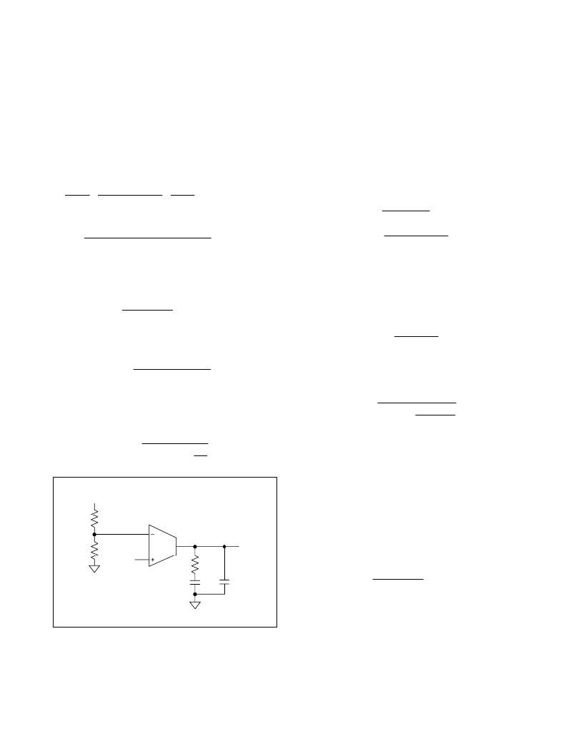
�Type� II� Compensation� Network�
�(Figure� 3)�
�If� f� ZO� is� lower� than� f� O� and� close� to� f� PO� ,� the� phase� lead� of�
�the� capacitor� ESR� zero� almost� cancels� the� phase� loss� of�
�one� of� the� complex� poles� of� the� LC� filter� around� the� cross-�
�over� frequency.� Use� a� Type� II� compensation� network� with�
�a� midband� zero� and� a� high-frequency� pole� to� stabilize�
�the� loop.� In� Figure� 3,� R� F� and� C� F� introduce� a� midband�
�zero� (f� Z1� ).� R� F� and� C� CF� in� the� Type� II� compensation� net-�
�work� provide� a� high-frequency� pole� (f� P1� ),� which� mitigates�
�the� effects� of� the� output� high-frequency� ripple.�
�Use� the� following� steps� to� calculate� the� component�
�values� for� Type� II� compensation� network� as� shown� in�
�Figure� 3:�
�1)� Calculate� the� gain� of� the� modulator� (GAIN� MOD� ),�
�comprised� of� the� regulator’s� pulse-width� modulator,�
�LC� filter,� feedback� divider,� and� associated� circuitry�
�at� crossover� frequency:�
�V� IN� ESR� V� FB�
�V� RAMP� (� 2� π� ×� f� O� ×� L� OUT� )� V� OUT�
�where� V� IN� is� the� input� voltage� of� the� regulator,� V� RAMP�
�is� the� amplitude� of� the� ramp� in� the� pulse-width� modula-�
�tor,� V� FB� is� the� FB� input� voltage� set� point� (0.6V� typically,�
�see� the� Electrical� Characteristics� table),� and� V� OUT� is� the�
�desired� output� voltage.�
�The� gain� of� the� error� amplifier� (GAIN� EA� )� in� midband�
�frequencies� is:�
�GAIN� EA� =� g� M� x� R� F�
�where� g� M� is� the� transconductance� of� the� error� amplifier.�
�Maxim� Integrated�
�相关PDF资料 |
PDF描述 |
|---|---|
| IR2111 | IC DRIVER HALF-BRIDGE 8-DIP |
| RJZ-0924S | CONV DC/DC 2W 09VIN 24VOUT |
| BAS70W-06-7 | DIODE SCHTKY CA 70V 200MW SC70-3 |
| VE-J3L-CW-F1 | CONVERTER MOD DC/DC 28V 100W |
| RCC05DRTN-S734 | CONN EDGECARD 10POS DIP .100 SLD |
相关代理商/技术参数 |
参数描述 |
|---|---|
| MAX15046BEVKIT+ | 功能描述:电源管理IC开发工具 MAX15046B Eval Kit RoHS:否 制造商:Maxim Integrated 产品:Evaluation Kits 类型:Battery Management 工具用于评估:MAX17710GB 输入电压: 输出电压:1.8 V |
| MAX15046CAEE+ | 功能描述:DC/DC 开关控制器 40V Synch Buck Controller RoHS:否 制造商:Texas Instruments 输入电压:6 V to 100 V 开关频率: 输出电压:1.215 V to 80 V 输出电流:3.5 A 输出端数量:1 最大工作温度:+ 125 C 安装风格: 封装 / 箱体:CPAK |
| MAX15046CAEE+T | 功能描述:DC/DC 开关控制器 40V Synch Buck Controller RoHS:否 制造商:Texas Instruments 输入电压:6 V to 100 V 开关频率: 输出电压:1.215 V to 80 V 输出电流:3.5 A 输出端数量:1 最大工作温度:+ 125 C 安装风格: 封装 / 箱体:CPAK |
| MAX15046EEE+ | 功能描述:DC/DC 开关控制器 RoHS:否 制造商:Texas Instruments 输入电压:6 V to 100 V 开关频率: 输出电压:1.215 V to 80 V 输出电流:3.5 A 输出端数量:1 最大工作温度:+ 125 C 安装风格: 封装 / 箱体:CPAK |
| MAX15046EEE+T | 功能描述:DC/DC 开关控制器 RoHS:否 制造商:Texas Instruments 输入电压:6 V to 100 V 开关频率: 输出电压:1.215 V to 80 V 输出电流:3.5 A 输出端数量:1 最大工作温度:+ 125 C 安装风格: 封装 / 箱体:CPAK |
发布紧急采购,3分钟左右您将得到回复。