- 您现在的位置:买卖IC网 > PDF目录20411 > MAX15046BEVKIT+ (Maxim Integrated)BOARD EVAL FOR MAX15046B PDF资料下载
参数资料
| 型号: | MAX15046BEVKIT+ |
| 厂商: | Maxim Integrated |
| 文件页数: | 8/24页 |
| 文件大小: | 0K |
| 描述: | BOARD EVAL FOR MAX15046B |
| 产品培训模块: | Lead (SnPb) Finish for COTS Obsolescence Mitigation Program |
| 标准包装: | 1 |
| 主要目的: | DC/DC,步降 |
| 输出及类型: | 1,非隔离 |
| 输出电压: | 3.3V |
| 电流 - 输出: | 10A |
| 输入电压: | 5 V ~ 40 V |
| 稳压器拓扑结构: | 降压 |
| 频率 - 开关: | 350kHz |
| 板类型: | 完全填充 |
| 已供物品: | 板 |
| 已用 IC / 零件: | MAX15046B |
�� �
�
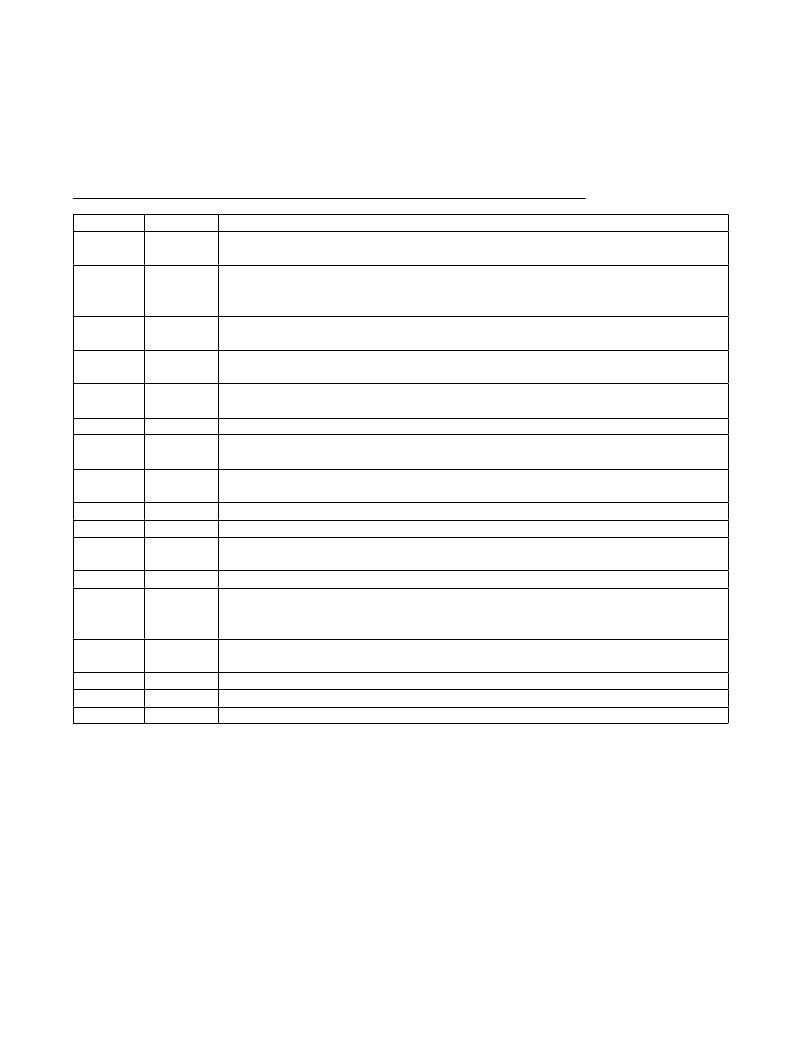
�MAX15046�
�40V,� High-Performance,� Synchronous�
�Buck� Controller�
�Pin� Description�
�8�
�PIN�
�1�
�2�
�3�
�4�
�5�
�6�
�7�
�8�
�9�
�10�
�11�
�12�
�13�
�14�
�15�
�16�
�—�
�NAME�
�IN�
�V� CC�
�PGOOD�
�EN�
�LIM�
�COMP�
�FB�
�RT�
�GND�
�PGND�
�DRV�
�DL�
�BST�
�LX�
�DH�
�CSP�
�EP�
�FUNCTION�
�Regulator� Input.� Connect� to� the� input� rail� of� the� buck� converter.� Bypass� IN� to� PGND� with� a� 100nF�
�minimum� ceramic� capacitor.� When� operating� in� the� 5V� Q� 10%� range,� connect� IN� to� V� CC� .�
�5.25V� Linear� Regulator� Output.� Bypass� V� CC� to� PGND� with� a� ceramic� capacitor� of� at� least� 4.7� F� F�
�when� V� CC� supplies� MOSFET� gate-driver� current� at� DRV� or� 2.2� F� F� when� V� CC� is� not� used� to� power�
�DRV.�
�Open-Drain� Power-Good� Output.� Pull� up� PGOOD� to� an� external� power� supply� or� output� with� an�
�external� resistor.�
�Active-High� Enable� Input.� Pull� EN� to� GND� to� disable� the� buck� converter� output.� Connect� to� V� CC�
�for always-on operation. EN can be used for power sequencing and as a UVLO adjustment input.�
�Current-Limit� Input.� Connect� a� resistor� from� LIM� to� GND� to� program� the� current-limit� threshold� from�
�30mV� (R� LIM� =� 6k� I� )� to� 300mV� (R� LIM� =� 60k� I� ).�
�Error-Amplifier� Output.� Connect� compensation� network� from� COMP� to� FB� or� from� COMP� to� GND.�
�Feedback� Input� (Inverting� Input� of� Error� Amplifier).� Connect� FB� to� a� resistive� divider� between� the�
�buck� converter� output� and� GND� to� adjust� the� output� voltage� from� 0.6V� up� to� 0.85� x� IN.�
�Oscillator-Timing� Resistor� Input.� Connect� a� resistor� from� RT� to� GND� to� set� the� oscillator� frequency�
�from� 100kHz� to� 1MHz.�
�Analog� Ground.� Connect� PGND� and� AGND� together� at� a� single� point.�
�Power� Ground.� Use� PGND� as� a� return� path� for� the� low-side� MOSFET� gate� driver.�
�Gate-Driver� Supply� Voltage.� DRV� is� internally� connected� to� the� low-side� driver� supply.� Bypass� DRV� to�
�PGND� with� a� 2.2� F� F� minimum� ceramic� capacitor� (see� the� Typical� Application� Circuits� ).�
�Low-Side� External� MOSFET� Gate-Driver� Output.� DL� swings� from� DRV� to� PGND.�
�Boost� Flying� Capacitor� Connection.� Internally� connected� to� the� high-side� driver� supply.� Connect� a�
�ceramic� capacitor� of� at� least� 100nF� between� BST� and� LX� and� a� diode� between� BST� and� DRV� for�
�the� high-side� MOSFET� gate-driver� supply.�
�Inductor� Connection.� Also� serves� as� a� return� terminal� for� the� high-side� MOSFET� driver� current.�
�Connect� LX� to� the� switching� side� of� the� inductor.�
�High-Side� External� MOSFET� Gate-Driver� Output.� DH� swings� from� BST� to� LX.�
�Current-Sense� Positive� Input.� Connect� to� the� drain� of� low-side� MOSFET� with� Kelvin� connection.�
�Exposed� Pad.� Connect� EP� to� a� large� copper� ground� plane� to� maximize� thermal� performance.�
�Maxim� Integrated�
�相关PDF资料 |
PDF描述 |
|---|---|
| IR2111 | IC DRIVER HALF-BRIDGE 8-DIP |
| RJZ-0924S | CONV DC/DC 2W 09VIN 24VOUT |
| BAS70W-06-7 | DIODE SCHTKY CA 70V 200MW SC70-3 |
| VE-J3L-CW-F1 | CONVERTER MOD DC/DC 28V 100W |
| RCC05DRTN-S734 | CONN EDGECARD 10POS DIP .100 SLD |
相关代理商/技术参数 |
参数描述 |
|---|---|
| MAX15046BEVKIT+ | 功能描述:电源管理IC开发工具 MAX15046B Eval Kit RoHS:否 制造商:Maxim Integrated 产品:Evaluation Kits 类型:Battery Management 工具用于评估:MAX17710GB 输入电压: 输出电压:1.8 V |
| MAX15046CAEE+ | 功能描述:DC/DC 开关控制器 40V Synch Buck Controller RoHS:否 制造商:Texas Instruments 输入电压:6 V to 100 V 开关频率: 输出电压:1.215 V to 80 V 输出电流:3.5 A 输出端数量:1 最大工作温度:+ 125 C 安装风格: 封装 / 箱体:CPAK |
| MAX15046CAEE+T | 功能描述:DC/DC 开关控制器 40V Synch Buck Controller RoHS:否 制造商:Texas Instruments 输入电压:6 V to 100 V 开关频率: 输出电压:1.215 V to 80 V 输出电流:3.5 A 输出端数量:1 最大工作温度:+ 125 C 安装风格: 封装 / 箱体:CPAK |
| MAX15046EEE+ | 功能描述:DC/DC 开关控制器 RoHS:否 制造商:Texas Instruments 输入电压:6 V to 100 V 开关频率: 输出电压:1.215 V to 80 V 输出电流:3.5 A 输出端数量:1 最大工作温度:+ 125 C 安装风格: 封装 / 箱体:CPAK |
| MAX15046EEE+T | 功能描述:DC/DC 开关控制器 RoHS:否 制造商:Texas Instruments 输入电压:6 V to 100 V 开关频率: 输出电压:1.215 V to 80 V 输出电流:3.5 A 输出端数量:1 最大工作温度:+ 125 C 安装风格: 封装 / 箱体:CPAK |
发布紧急采购,3分钟左右您将得到回复。