- 您现在的位置:买卖IC网 > PDF目录20411 > MAX15046BEVKIT+ (Maxim Integrated)BOARD EVAL FOR MAX15046B PDF资料下载
参数资料
| 型号: | MAX15046BEVKIT+ |
| 厂商: | Maxim Integrated |
| 文件页数: | 2/24页 |
| 文件大小: | 0K |
| 描述: | BOARD EVAL FOR MAX15046B |
| 产品培训模块: | Lead (SnPb) Finish for COTS Obsolescence Mitigation Program |
| 标准包装: | 1 |
| 主要目的: | DC/DC,步降 |
| 输出及类型: | 1,非隔离 |
| 输出电压: | 3.3V |
| 电流 - 输出: | 10A |
| 输入电压: | 5 V ~ 40 V |
| 稳压器拓扑结构: | 降压 |
| 频率 - 开关: | 350kHz |
| 板类型: | 完全填充 |
| 已供物品: | 板 |
| 已用 IC / 零件: | MAX15046B |
�� �
�
�MAX15046�
�40V,� High-Performance,� Synchronous�
�Buck� Controller�
�ABSOLUTE� MAXIMUM� RATINGS�
�IN� to� GND� ..............................................................-0.3V� to� +45V�
�V� CC� to� GND.....................� -0.3V� to� lower� of� (V� IN� +� 0.6V)� and� 6V�
�EN,� DRV� to� GND� .....................................................-0.3V� to� +6V�
�PGOOD� to� GND� ....................................................-0.3V� to� +45V�
�PGND� to� GND� ......................................................-0.3V� to� +0.3V�
�DL� to� PGND.............................................-0.3V� to� (V� DRV� +� 0.3V)�
�BST� to� PGND� .......................................................-0.3V� to� +50V�
�LX� and� CSP� to� PGND...............................................-1V� to� +45V�
�LX� and� CSP� to� PGND............................-2V� (50ns� max)� to� +45V�
�BST� to� LX.................................................................-0.3V� to� +6V�
�CSP� to� LX� .............................................................-0.3V� to� +0.3V�
�All� Other� Pins� to� GND� ..............................� -0.3V� to� (V� CC� +� 0.3V)�
�V� CC� Short� Circuit� to� GND..........................................Continuous�
�PGOOD� Maximum� Sink� Current� .........................................20mA�
�Continuous� Power� Dissipation� (T� A� =� +70� N� C):�
�16-Pin� QSOP� (derate� 9.6mW/� N� C� above� +70� N� C)� .......771.5mW�
�16-Pin� QSOP-EP� (derate� 22.7mW/� N� C� above� +70� N� C)� 1818.2mW�
�Operating� Temperature� Range� ........................� -40� N� C� to� +125� N� C�
�Junction� Temperature� .....................................................+150� N� C�
�Storage� Temperature� Range............................� -65� N� C� to� +150� N� C�
�Lead� Temperature� (soldering,� 10s)� ................................+300� N� C�
�Soldering� Temperature� (reflow)� ......................................+260� N� C�
�DH� to� LX� ..................................................� -0.3V� to� (V� BST� +� 0.3V)�
�Stresses� beyond� those� listed� under� “Absolute� Maximum� Ratings”� may� cause� permanent� damage� to� the� device.� These� are� stress� ratings� only,� and� functional�
�operation� of� the� device� at� these� or� any� other� conditions� beyond� those� indicated� in� the� operational� sections� of� the� specifications� is� not� implied.� Exposure� to� absolute�
�maximum� rating� conditions� for� extended� periods� may� affect� device� reliability.�
�PACKAGE� THERMAL� CHARACTERISTICS� (Note� 1)�
�QSOP�
�Junction-to-Ambient� Thermal� Resistance� (� q� JA� )� ....� +103.7°C/W�
�Junction-to-Case� Thermal� Resistance� (� q� JC� )� ..............� +37°C/W�
�QSOP-EP�
�Junction-to-Ambient� Thermal� Resistance� (� q� JA� )� .........� +44°C/W�
�Junction-to-Case� Thermal� Resistance� (� q� JC� )� ................� +6°C/W�
�Note� 1:� Package� thermal� resistances� were� obtained� using� the� method� described� in� JEDEC� specification� JESD51-7,� using� a� four-layer�
�board.� For� detailed� information� on� package� thermal� considerations,� refer� to� http://www.maximintegrated.com/thermal-tutorial� .�
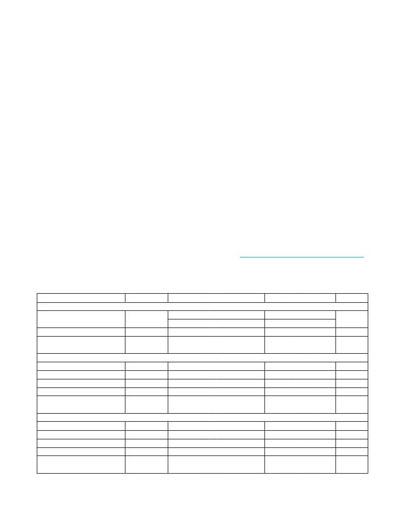
�ELECTRICAL� CHARACTERISTICS�
�(V� IN� =� 24V,� V� EN� =� 5V,� V� GND� =� V� PGND� =� 0V,� C� IN� =� 1� F� F,� C� VCC� =� 4.7� F� F,� R� RT� =� 49.9k� I� ,� T� A� =� T� J� =� -40� N� C� to� +125� N� C,� unless� otherwise�
�noted.� Typical� values� are� at� T� A� =� +25� N� C.)� (Note� 2)�
�PARAMETER�
�SYMBOL�
�CONDITIONS�
�MIN�
�TYP�
�MAX�
�UNITS�
�SYSTEM� SPECIFICATIONS�
�Input-Voltage� Range�
�Quiescent� Supply� Current�
�Shutdown� Supply� Current�
�V� IN�
�I� IN_Q�
�I� IN_SBY�
�V� IN� =� V� CC� =� V� DRV�
�V� IN� = 24V, V� FB� =� 0.9V,� no� switching�
�V� IN� =� 24V,� V� EN� =� 0V,� I� VCC� =� 0,�
�PGOOD� =� unconnected�
�4.5�
�4.5�
�2�
�0.35�
�40�
�5.5�
�3�
�0.55�
�V�
�mA�
�mA�
�V� CC� REGULATOR�
�Output� Voltage�
�V� CC� Regulator� Dropout�
�V� CC� Short-Circuit� Output� Current�
�V� CC� Undervoltage� Lockout�
�V� CC�
�V� CCUVLO�
�6V ≤ V� IN� ≤ 40V,� I� LOAD� =� 6mA�
�V� IN� =� 4.5V,� I� LOAD� =� 25mA�
�V� IN� =� 5V�
�V� CC� rising�
�5�
�30�
�3.8�
�5.25�
�0.18�
�55�
�4�
�5.5�
�0.45�
�90�
�4.2�
�V�
�V�
�mA�
�V�
�V� CC� Undervoltage� Lockout�
�Hysteresis�
�ERROR AMPLIFIER (FB, COMP)�
�400�
�mV�
�FB� Input-Voltage� Set� Point�
�V� FB�
�584�
�590�
�596�
�mV�
�FB� Input� Bias� Current�
�I� FB�
�V� FB� =� 0.6V�
�-250�
�+250�
�nA�
�FB� to� COMP� Transconductance�
�g� M�
�I� COMP� =� Q� 20� F� A�
�600�
�1200�
�1800�
�F� S�
�Open-Loop� Gain�
�80�
�dB�
�Unity-Gain� Bandwidth�
�2�
�Capacitor� from� COMP� to� GND� =�
�47pF�
�5�
�MHz�
�Maxim� Integrated�
�相关PDF资料 |
PDF描述 |
|---|---|
| IR2111 | IC DRIVER HALF-BRIDGE 8-DIP |
| RJZ-0924S | CONV DC/DC 2W 09VIN 24VOUT |
| BAS70W-06-7 | DIODE SCHTKY CA 70V 200MW SC70-3 |
| VE-J3L-CW-F1 | CONVERTER MOD DC/DC 28V 100W |
| RCC05DRTN-S734 | CONN EDGECARD 10POS DIP .100 SLD |
相关代理商/技术参数 |
参数描述 |
|---|---|
| MAX15046BEVKIT+ | 功能描述:电源管理IC开发工具 MAX15046B Eval Kit RoHS:否 制造商:Maxim Integrated 产品:Evaluation Kits 类型:Battery Management 工具用于评估:MAX17710GB 输入电压: 输出电压:1.8 V |
| MAX15046CAEE+ | 功能描述:DC/DC 开关控制器 40V Synch Buck Controller RoHS:否 制造商:Texas Instruments 输入电压:6 V to 100 V 开关频率: 输出电压:1.215 V to 80 V 输出电流:3.5 A 输出端数量:1 最大工作温度:+ 125 C 安装风格: 封装 / 箱体:CPAK |
| MAX15046CAEE+T | 功能描述:DC/DC 开关控制器 40V Synch Buck Controller RoHS:否 制造商:Texas Instruments 输入电压:6 V to 100 V 开关频率: 输出电压:1.215 V to 80 V 输出电流:3.5 A 输出端数量:1 最大工作温度:+ 125 C 安装风格: 封装 / 箱体:CPAK |
| MAX15046EEE+ | 功能描述:DC/DC 开关控制器 RoHS:否 制造商:Texas Instruments 输入电压:6 V to 100 V 开关频率: 输出电压:1.215 V to 80 V 输出电流:3.5 A 输出端数量:1 最大工作温度:+ 125 C 安装风格: 封装 / 箱体:CPAK |
| MAX15046EEE+T | 功能描述:DC/DC 开关控制器 RoHS:否 制造商:Texas Instruments 输入电压:6 V to 100 V 开关频率: 输出电压:1.215 V to 80 V 输出电流:3.5 A 输出端数量:1 最大工作温度:+ 125 C 安装风格: 封装 / 箱体:CPAK |
发布紧急采购,3分钟左右您将得到回复。