- 您现在的位置:买卖IC网 > PDF目录11790 > MAX1840EUB+ (Maxim Integrated Products)IC TRANS LEVEL SIM 10-UMAX PDF资料下载
参数资料
| 型号: | MAX1840EUB+ |
| 厂商: | Maxim Integrated Products |
| 文件页数: | 6/8页 |
| 文件大小: | 0K |
| 描述: | IC TRANS LEVEL SIM 10-UMAX |
| 产品培训模块: | Lead (SnPb) Finish for COTS Obsolescence Mitigation Program |
| 标准包装: | 50 |
| 应用: | 智能卡 |
| 接口: | MICROWIRE?,QSPI?,串行,SPI? |
| 电源电压: | 1.4 V ~ 5.5 V,1.7 V ~ 5.5 V |
| 封装/外壳: | 10-TFSOP,10-MSOP(0.118",3.00mm 宽) |
| 供应商设备封装: | 10-µMAX |
| 包装: | 管件 |
| 安装类型: | 表面贴装 |
| 产品目录页面: | 1410 (CN2011-ZH PDF) |
MAX1840/MAX1841
Low-Voltage SIM/Smart Card
Level Translators in MAX
6
_______________________________________________________________________________________
Detailed Description
The MAX1840/MAX1841 provide the necessary level
translation for interfacing with SIMs and smart cards in
multivoltage systems. These devices operate with logic
supply voltages between +1.4V and +5.5V on the con-
troller side (DVCC) and between +1.7V and +5.5V on the
card side (VCC). The total supply current (IDVCC + IVCC)
is 1A while operating in an idle state (see Electrical
Characteristics). Figure 1 shows the MAX1840/MAX1841
test circuit. The Typical Application Circuit appears at the
end of this data sheet.
Level Translation
The MAX1840/MAX1841 provide level translators for a
clock input, a reset input, and a bidirectional data IO.
The clock and reset inputs (CIN and RIN) are level shift-
ed from the controller-side supply rails (DVCC to GND)
to the card-side supply rails (VCC to GND). When con-
nected to an open-drain controller output, DATA and IO
provide bidirectional level translation. All level transla-
tion is valid for DVCC
≥ VCC or DVCC ≤ VCC. The
MAX1840/MAX1841 contain internal pull up resistors
from DATA to the controller-side supply (DVCC) and
from IO to the card-side supply (VCC). For push-pull
controller outputs, see the Data Driver section for bidi-
rectional data translation.
Data Driver (MAX1841 Only)
When using a microcontroller (C) without an open-drain
output, use the data driver (DDRV) input to send data to
the SIM/smart card, while DATA provides the controller-
side output for bidirectional data transfer. When not
used, connect DDRV to DVCC to reduce total supply cur-
rent.
Shutdown Mode
For the MAX1840, drive SHDN low to activate shut-
down. Connect SHDN to DVCC or drive high for normal
operation. To allow for card insertion and removal, shut-
down mode actively pulls CLK, RST, and IO low; it also
disconnects the internal 10k
pull up resistor from VCC
to prevent excessive current draw. Shutdown mode
reduces the total supply current (IDVCC + IVCC) to
0.01A.
SIM/Smart Card Insertion/Removal
The SIM/smart card specifications require that the card-
side pins (VCC, CLK, RST, IO) be at ground potential
prior to inserting the SIM/smart card. For applications
using the MAX1686H (Figure 3), the easiest way to
achieve this is by shutting down the MAX1686H or by
driving SHDN (MAX1840 only) low. If specific sequenc-
ing is desired, pull IO low by driving either DATA or
DDRV (MAX1841 only) low, and pull CLK and RST low
by driving CIN and RIN low, respectively.
ESD Protection
As with all Maxim devices, ESD-protection structures on
all pins protect against ESDs encountered during han-
dling and assembly. For further protection during card
insertion and removal, the pins that connect to the card
socket (CLK, RST, IO, VCC, and GND) provide protec-
tion against ±10kV of ESD. The ESD structures with-
stand high ESD in all states: normal operation,
shutdown, and power-down. After an ESD event, the
MAX1840/MAX1841 continue working without latchup.
A 1F bypass capacitor from VCC to GND is required to
exceed ±10kV ESD specifications.
ESD Test Conditions
ESD performance depends on a variety of conditions.
Contact Maxim for a reliability report documenting test
setup, test methodology, and test results.
Applications Information
SIM/Smart Card Interface
To provide 5V when interfacing with a 5V SIM/smart card,
+3V systems require a DC-DC converter. The MAX1686H
+5V regulating charge pump for SIM cards provides
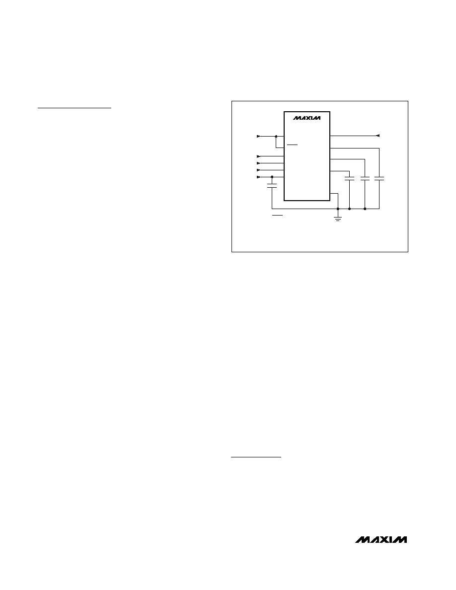
GND
IO
CLK
RST
VCC
DVCC
+1.8V
+1.8V,
+3.0V, OR
+5.0V
30pF
MAX1840
MAX1841
SHDN*
RIN
CIN
DDRV*
DATA
SHDN FOR MAX1840 ONLY;
DDRV FOR MAX1841 ONLY.
*
NOTE: ALL CAPACITANCES INCLUDE CAPACITIVE LOADS OF
TEST PROBES AND BOARD LAYOUT.
Figure 1. MAX1840/MAX1841 Test Circuit
相关PDF资料 |
PDF描述 |
|---|---|
| VI-BTH-IX-F2 | CONVERTER MOD DC/DC 52V 75W |
| DS8023-RJX+ | IC INTERFACE SMART CARD 28-TSSOP |
| VI-BTH-IX-F1 | CONVERTER MOD DC/DC 52V 75W |
| VI-BTH-IW-F3 | CONVERTER MOD DC/DC 52V 100W |
| NCN6000DTBR2 | IC INTERFACE SMART CARD 20TSSOP |
相关代理商/技术参数 |
参数描述 |
|---|---|
| MAX1840EUB+ | 功能描述:转换 - 电压电平 SIM/Smart-Card Level Translator RoHS:否 制造商:Micrel 类型:CML/LVDS/LVPECL to LVCMOS/LVTTL 传播延迟时间:1.9 ns 电源电流:14 mA 电源电压-最大:3.6 V 电源电压-最小:3 V 最大工作温度:+ 85 C 安装风格:SMD/SMT 封装 / 箱体:MLF-8 |
| MAX1840EUB+T | 功能描述:转换 - 电压电平 SIM/Smart-Card Level Translator RoHS:否 制造商:Micrel 类型:CML/LVDS/LVPECL to LVCMOS/LVTTL 传播延迟时间:1.9 ns 电源电流:14 mA 电源电压-最大:3.6 V 电源电压-最小:3 V 最大工作温度:+ 85 C 安装风格:SMD/SMT 封装 / 箱体:MLF-8 |
| MAX1840EUB-T | 功能描述:转换 - 电压电平 SIM/Smart-Card Level Translator RoHS:否 制造商:Micrel 类型:CML/LVDS/LVPECL to LVCMOS/LVTTL 传播延迟时间:1.9 ns 电源电流:14 mA 电源电压-最大:3.6 V 电源电压-最小:3 V 最大工作温度:+ 85 C 安装风格:SMD/SMT 封装 / 箱体:MLF-8 |
| MAX1841EUB | 功能描述:转换 - 电压电平 SIM/Smart-Card Level Translator RoHS:否 制造商:Micrel 类型:CML/LVDS/LVPECL to LVCMOS/LVTTL 传播延迟时间:1.9 ns 电源电流:14 mA 电源电压-最大:3.6 V 电源电压-最小:3 V 最大工作温度:+ 85 C 安装风格:SMD/SMT 封装 / 箱体:MLF-8 |
| MAX1841EUB+ | 功能描述:转换 - 电压电平 SIM/Smart-Card Level Translator RoHS:否 制造商:Micrel 类型:CML/LVDS/LVPECL to LVCMOS/LVTTL 传播延迟时间:1.9 ns 电源电流:14 mA 电源电压-最大:3.6 V 电源电压-最小:3 V 最大工作温度:+ 85 C 安装风格:SMD/SMT 封装 / 箱体:MLF-8 |
发布紧急采购,3分钟左右您将得到回复。