- 您现在的位置:买卖IC网 > PDF目录16798 > MAX1864TEEE+ (Maxim Integrated Products)IC PWR SUPPLY CONTROLLER 16QSOP PDF资料下载
参数资料
| 型号: | MAX1864TEEE+ |
| 厂商: | Maxim Integrated Products |
| 文件页数: | 13/25页 |
| 文件大小: | 0K |
| 描述: | IC PWR SUPPLY CONTROLLER 16QSOP |
| 产品培训模块: | Lead (SnPb) Finish for COTS Obsolescence Mitigation Program |
| 标准包装: | 100 |
| 应用: | 电源控制器 |
| 输入电压: | 4.5 V ~ 28 V |
| 电流 - 电源: | 1mA |
| 工作温度: | -40°C ~ 85°C |
| 安装类型: | 表面贴装 |
| 封装/外壳: | 16-SSOP(0.154",3.90mm 宽) |
| 供应商设备封装: | 16-QSOP |
| 包装: | 管件 |
�� �
�
�xDSL/Cable� Modem� Triple/Quintuple� Output�
�Power� Supplies�
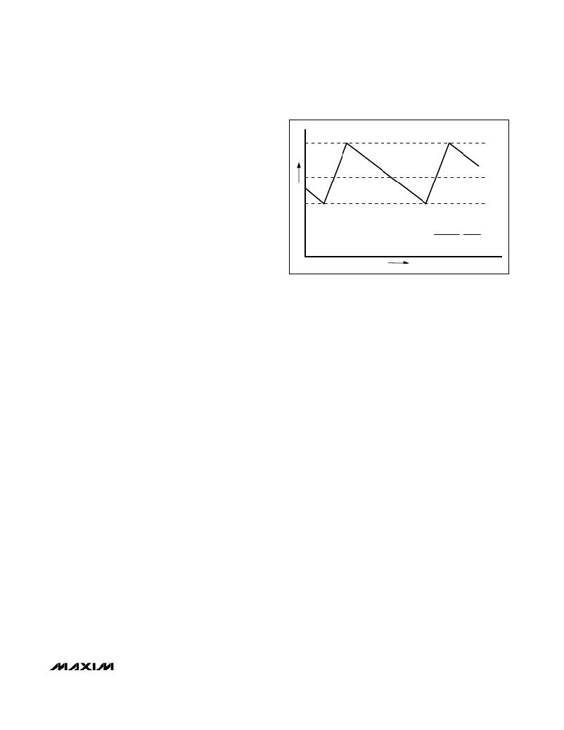
�Current-Limit� Circuit�
�The� current-limit� circuit� employs� a� unique� “valley”� cur-�
�rent-limiting� algorithm� that� uses� the� low-side� MOSFET’s�
�on-resistance� as� a� sensing� element� (Figure� 3).� If� the�
�voltage� across� the� low-side� MOSFET� (R� DS(ON)� ?� I� IN-�
�DUCTOR� )� exceeds� the� current-limit� threshold� at� the�
�beginning� of� a� new� oscillator� cycle,� the� MAX1864/�
�MAX1865� will� not� turn� on� the� high-side� MOSFET.� The�
�actual� peak� current� is� greater� than� the� current-limit�
�threshold� by� an� amount� equal� to� the� inductor� ripple�
�-I� PEAK�
�I� LOAD�
�I� VALLEY�
�[�
�(� )� ]�
�current.� Therefore,� the� exact� current-limit� characteristic�
�and� maximum� load� capability� are� a� function� of� the� low-�
�side� MOSFET� on-resistance,� inductor� value,� input� volt-�
�I� PEAK� =� I� VALLEY� +�
�(V� IN� -� V� OUT� )�
�L�
�V� OUT�
�V� IN� f� OSC�
�age,� and� output� voltage.� The� reward� for� this� uncertainty�
�is� robust,� loss-less� overcurrent� limiting.�
�In� adjustable� mode,� the� current-limit� threshold� voltage�
�is� 1/5th� the� voltage� seen� at� ILIM� (I� VALLEY� =� 0.2� ?� V� ILIM� ).�
�Adjust� the� current-limit� threshold� by� connecting� a� resis-�
�tive-divider� from� VL� to� ILIM� to� GND.� The� current-limit�
�threshold� can� be� set� from� 106mV� to� 530mV,� which� cor-�
�responds� to� ILIM� input� voltages� of� 500mV� to� 2.5V.� This�
�adjustable� current� limit� accommodates� MOSFETs� with�
�a� wide� range� of� on-resistance� characteristics� (see�
�Design� Procedure� ).� The� current-limit� threshold� defaults�
�to� 250mV� when� ILIM� is� connected� to� VL.� The� logic�
�threshold� for� switchover� to� the� 250mV� default� value� is�
�approximately� VL� -� 1V.�
�Carefully� observe� the� PC� board� layout� guidelines� to�
�ensure� that� noise� and� DC� errors� don’t� corrupt� the� cur-�
�rent-sense� signals� seen� by� LX� and� GND.� The� IC� must�
�be� mounted� close� to� the� low-side� MOSFET� with� short�
�(less� than� 5mm),� direct� traces� making� a� Kelvin� sense�
�connection.�
�Synchronous� Rectifier� Driver� (DL)�
�Synchronous� rectification� reduces� conduction� losses� in�
�the� rectifier� by� replacing� the� normal� Schottky� catch�
�diode� with� a� low-resistance� MOSFET� switch.� The�
�MAX1864/MAX1865� also� use� the� synchronous� rectifier�
�to� ensure� proper� startup� of� the� boost� gate-driver� circuit�
�and� to� provide� the� current-limit� signal.�
�The� DL� low-side� drive� waveform� is� always� the� comple-�
�ment� of� the� DH� high-side� drive� waveform� (with� con-�
�trolled� dead� time� to� prevent� cross-conduction� or�
�“shoot-through”).� A� dead-time� circuit� monitors� the� DL�
�output� and� prevents� the� high-side� FET� from� turning� on�
�until� DL� is� fully� off.� For� the� dead-time� circuit� to� work�
�properly,� there� must� be� a� low-resistance,� low-induc-�
�tance� path� from� the� DL� driver� to� the� MOSFET� gate.�
�Otherwise,� the� sense� circuitry� in� the� MAX1864/�
�MAX1865� will� interpret� the� MOSFET� gate� as� “off”� when�
�gate� charge� actually� remains.� Use� very� short,� wide�
�TIME�
�Figure� 3.� “Valley”� Current-Limit� Threshold� Point�
�traces� (50mil� to� 100mil� wide� if� the� MOSFET� is� 1� inch�
�from� the� device).� The� dead� time� at� the� other� edge� (DH�
�turning� off)� is� determined� by� a� fixed� internal� delay.�
�High-Side� Gate-Drive� Supply� (BST)�
�Gate-drive� voltage� for� the� high-side� N-channel� switch� is�
�generated� by� a� flying-capacitor� boost� circuit� (Figure� 1).�
�The� capacitor� between� BST� and� LX� is� alternately�
�charged� from� the� VL� supply� and� placed� parallel� to� the�
�high-side� MOSFET’s� gate-source� terminals.�
�On� startup,� the� synchronous� rectifier� (low-side� MOS-�
�FET)� forces� LX� to� ground� and� charges� the� boost�
�capacitor� to� 5V.� On� the� second� half-cycle,� the� switch-�
�mode� power� supply� turns� on� the� high-side� MOSFET� by�
�closing� an� internal� switch� between� BST� and� DH.� This�
�provides� the� necessary� gate-to-source� voltage� to� turn�
�on� the� high-side� switch,� an� action� that� boosts� the� 5V�
�gate-drive� signal� above� the� battery� voltage.�
�Internal� 5V� Linear� Regulator� (VL)�
�All� MAX1864/MAX1865� functions,� except� the� current-�
�sense� amplifier,� are� internally� powered� from� the� on-�
�chip,� low-dropout� 5V� regulator.� The� maximum� regulator�
�input� voltage� (V� IN� )� is� 28V.� Bypass� the� regulator’s� output�
�(VL)� with� at� least� a� 1μF� ceramic� capacitor� to� GND.� The�
�V� IN� -to-VL� dropout� voltage� is� typically� 200mV,� so� when�
�V� IN� is� less� than� 5.2V,� VL� is� typically� V� IN� -� 200mV.�
�The� internal� linear� regulator� can� source� up� to� 20mA� to�
�supply� the� IC,� power� the� low-side� gate� driver,� charge�
�the� external� boost� capacitor,� and� supply� small� external�
�loads.� When� driving� particularly� large� FETs,� little� or� no�
�regulator� current� may� be� available� for� external� loads.�
�For� example,� when� switched� at� 200kHz,� a� large� FET�
�with� 40nC� total� gate� charge� requires� 40nC� x� 200kHz,�
�or� 8mA.�
�______________________________________________________________________________________�
�13�
�相关PDF资料 |
PDF描述 |
|---|---|
| RNF-100-1/16-CL-SP | HEAT SHRINK TUBING |
| GBC20DRTH-S734 | CONN EDGECARD 40POS DIP .100 SLD |
| H6MMH-1636M | DIP CABLE - HDM16H/AE16M/HDM16H |
| 0982661101 | CBL 39POS 0.5MM JMPR TYPE A 3" |
| V300B3V3E100BG3 | CONVERTER MOD DC/DC 3.3V 100W |
相关代理商/技术参数 |
参数描述 |
|---|---|
| MAX1864TEEE+ | 功能描述:DC/DC 开关控制器 xDSL/Cable Modem Triple/Quint Output RoHS:否 制造商:Texas Instruments 输入电压:6 V to 100 V 开关频率: 输出电压:1.215 V to 80 V 输出电流:3.5 A 输出端数量:1 最大工作温度:+ 125 C 安装风格: 封装 / 箱体:CPAK |
| MAX1864TEEE+T | 功能描述:电流和电力监控器、调节器 xDSL/Cable Modem Triple/Quint Output RoHS:否 制造商:STMicroelectronics 产品:Current Regulators 电源电压-最大:48 V 电源电压-最小:5.5 V 工作温度范围:- 40 C to + 150 C 安装风格:SMD/SMT 封装 / 箱体:HPSO-8 封装:Reel |
| MAX1864TEEE-T | 功能描述:电流和电力监控器、调节器 RoHS:否 制造商:STMicroelectronics 产品:Current Regulators 电源电压-最大:48 V 电源电压-最小:5.5 V 工作温度范围:- 40 C to + 150 C 安装风格:SMD/SMT 封装 / 箱体:HPSO-8 封装:Reel |
| MAX1864UEEE | 功能描述:电流和电力监控器、调节器 RoHS:否 制造商:STMicroelectronics 产品:Current Regulators 电源电压-最大:48 V 电源电压-最小:5.5 V 工作温度范围:- 40 C to + 150 C 安装风格:SMD/SMT 封装 / 箱体:HPSO-8 封装:Reel |
| MAX1864UEEE-T | 功能描述:电流和电力监控器、调节器 RoHS:否 制造商:STMicroelectronics 产品:Current Regulators 电源电压-最大:48 V 电源电压-最小:5.5 V 工作温度范围:- 40 C to + 150 C 安装风格:SMD/SMT 封装 / 箱体:HPSO-8 封装:Reel |
发布紧急采购,3分钟左右您将得到回复。