- 您现在的位置:买卖IC网 > PDF目录1841 > MAX1956ETI+T (Maxim Integrated Products)IC REG CTRLR BUCK PWM VM 28-TQFN PDF资料下载
参数资料
| 型号: | MAX1956ETI+T |
| 厂商: | Maxim Integrated Products |
| 文件页数: | 13/22页 |
| 文件大小: | 0K |
| 描述: | IC REG CTRLR BUCK PWM VM 28-TQFN |
| 产品培训模块: | Lead (SnPb) Finish for COTS Obsolescence Mitigation Program |
| 标准包装: | 2,500 |
| PWM 型: | 电压模式 |
| 输出数: | 2 |
| 频率 - 最大: | 660kHz |
| 占空比: | 97% |
| 电源电压: | 1.6 V ~ 5.5 V |
| 降压: | 是 |
| 升压: | 无 |
| 回扫: | 无 |
| 反相: | 无 |
| 倍增器: | 无 |
| 除法器: | 无 |
| Cuk: | 无 |
| 隔离: | 无 |
| 工作温度: | -40°C ~ 85°C |
| 封装/外壳: | 28-WFQFN 裸露焊盘 |
| 包装: | 带卷 (TR) |
�� �
�
�1.6V� to� 5.5V� Input,� 0.5%� Accurate,� Dual�
�180°� Out-of-Phase� Step-Down� Controllers�
�Synchronization�
�An� external� clock� of� 1080kHz� to� 1320kHz� at� SYNC�
�forces� the� controller� to� switch� at� half� of� this� clock� fre-�
�quency.� DH1� and� DH2� positive-going� edges� alternately�
�synchronize� to� the� rising� edge� of� the� external� clock,�
�thus� operating� 180� °� out-of-phase� with� each� other.� See�
�the� Synchronization� and� Switching� Waveforms� in� the�
�Typical� Operating� Characteristics� .�
�Shutdown� and� Output� Voltage�
�Margining� (EN)�
�The� MAX1955/MAX1956� feature� a� low-power� shutdown�
�mode� that� reduces� the� IC� ’� s� current� consumption� to� less�
�than� 20μA.� For� normal� operation,� connect� EN� to� IN.� To�
�place� the� part� in� low-current� shutdown� mode,� connect�
�EN� to� GND.�
�When� the� MAX1955/MAX1956� enter� shutdown� (EN�
�goes� low),� soft-stop� begins.� In� soft-stop,� the� output� volt-�
�age� is� ramped� down� by� lowering� the� FB_� regulation�
�voltage� to� zero� in� 80� steps� of� 10mV.� Total� soft-stop� time�
�is� typically� 4.27ms.�
�Each� controller� can� be� shut� down� individually� by�
�pulling� COMP_� to� GND� with� an� open� collector� NPN�
�transistor� (Figure� 6).� This� shuts� down� the� controller�
�immediately� without� going� through� soft-stop.� Once�
�COMP_� is� released,� the� controller� powers� up� without�
�going� through� soft-start.� To� protect� against� inrush� cur-�
�rent� when� using� this� power-up/-down� method,� use� fold-�
�back� current� limit.� Also,� connect� SEQ� to� GND� to�
�prevent� output� 2� from� powering� down� when� the� voltage�
�on� output� 1� drops.�
�In� an� effort� to� improve� quality,� many� OEMs� are� testing�
�their� system� ’� s� operation� over� the� range� of� minimum� and�
�maximum� supply� voltage.� To� facilitate� this� testing,� the�
�MAX1955/MAX1956� have� a� voltage-margining� feature�
�that� increases� or� decreases� the� output� voltages� by� 4%.�
�The� voltage� on� EN� controls� voltage� margining.� To�
�increase� the� output� voltage� by� 4%,� apply� (2/3)� V� IN� to� EN.�
�To� reduce� the� output� voltage� by� 4%,� apply� (1/3)� V� IN� to� EN.�
�Thermal-Overload� Protection�
�Thermal-overload� protection� limits� total� power� dissipa-�
�tion� of� the� MAX1955/MAX1956.� When� the� junction� tem-�
�perature� exceeds� +160� °� C,� an� internal� thermal� sensor�
�shuts� down� the� device,� allowing� the� IC� to� cool.� The�
�thermal� sensor� turns� the� device� on� after� the� junction�
�temperature� cools� by� 15� °� C.� In� a� continuous� thermal-�
�overload� condition,� this� results� in� a� pulsed� output.�
�Low-Side� MOSFET� Negative-�
�Current� Conduction�
�Under� most� operating� conditions,� the� low-side� MOSFET�
�conducts� only� positive� inductor� currents� that� flow� from�
�source� to� drain� and� 1/2� of� the� inductor� peak-to-peak�
�ripple� current� (~15%� full� load� current)� in� the� negative�
�direction� when� output� is� at� no� load.� If� the� MAX1955/�
�MAX1956� are� disabled� before� their� soft-start� cycle� is�
�complete� (~4ms),� the� converter� is� disabled� without� a�
�soft-stop,� and� the� output� discharges� through� its� load.� In�
�this� case,� if� the� converter� is� reenabled� before� the� out-�
�put� capacitor� discharges� completely,� the� soft-start�
�cycle� resets� the� reference� input� to� the� error� amp� to� zero�
�and� ramps� up� again.�
�The� converter� forces� DL� on� until� the� feedback� drops�
�below� the� reference� input.� If� the� output� is� almost� fully�
�charged� when� the� converter� turns� back� on,� a� large�
�negative� current� can� build� up� in� the� inductor.� If� the�
�negative� current� is� excessive,� a� high� LX� voltage� spike�
�can� occur� because� of� parasitic� circuit� inductances� as�
�DL� is� released.� This� high� LX� voltage� spike� can� shut�
�down� and� latch� off� the� circuit.� To� prevent� this� from� hap-�
�pening,� add� a� series� resistor� between� DL� and� the� gate�
�of� the� low-side� MOSFET� (Figure� 6)� to� slow� down� the�
�turn-off� di/dt,� reducing� the� voltage� spike� and� prevent-�
�ing� the� circuit� from� shutting� down.� A� 1� ?� resistor� works�
�fine� for� most� applications� without� noticeable� degrading�
�impact� on� efficiency� or� Cdv/dt-induced� turn-on� effect.�
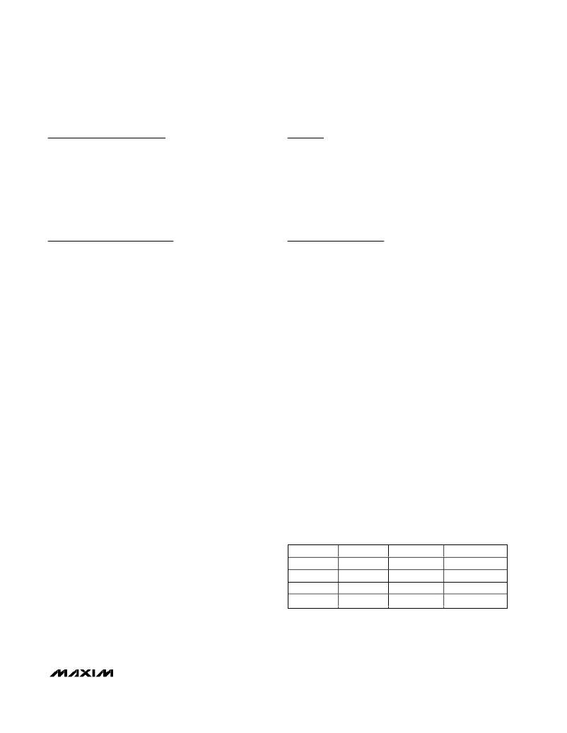
�Table� 1.� Voltage� Margining�
�One� easy� way� to� use� the� voltage-margining� feature� is� to�
�make� two� control� logic� inputs� (CTL1� and� CTL2)� by� con-�
�necting� two� resistors� to� EN.� Connect� a� 200k� ?� resistor�
�from� EN� to� CTL1,� and� a� 100k� ?� resistor� from� EN� to� CTL2�
�(Figure� 5).� The� voltage� margining� is� then� controlled� by�
�connecting� CTL1� and� CTL2� to� IN� or� GND,� as� shown� in�
�Table� 1.� Before� applying� voltage-margining,� pull� VCTL1�
�CTL1�
�V� IN�
�0�
�V� IN�
�0�
�CTL2�
�V� IN�
�V� IN�
�0�
�0�
�EN�
�V� IN�
�(2/3)V� IN�
�(1/3)V� IN�
�0�
�OUTPUT�
�Nominal�
�+4%�
�-4%�
�Shutdown�
�and� VCTL2� to� >� V� IN� -� 0.5V� to� ensure� proper� startup.�
�______________________________________________________________________________________�
�13�
�相关PDF资料 |
PDF描述 |
|---|---|
| MAX1961EEP+ | IC REG CTRLR BUCK PWM VM 20-QSOP |
| MAX1964TEEE+ | IC POWER CTRLR/SEQUENCER 16QSOP |
| MAX1967EUB+T | IC REG CTRLR BUCK PWM VM 10-UMAX |
| MAX1969EUI+T | IC DRVR POWER 28-TSSOP |
| MAX1971EEE+T | IC REG BUCK SYNC 0.75A DL 16QSOP |
相关代理商/技术参数 |
参数描述 |
|---|---|
| MAX1957EUB | 功能描述:电流型 PWM 控制器 RoHS:否 制造商:Texas Instruments 开关频率:27 KHz 上升时间: 下降时间: 工作电源电压:6 V to 15 V 工作电源电流:1.5 mA 输出端数量:1 最大工作温度:+ 105 C 安装风格:SMD/SMT 封装 / 箱体:TSSOP-14 |
| MAX1957EUB+ | 功能描述:电流型 PWM 控制器 High-f Current-Mode PWM Buck Controller RoHS:否 制造商:Texas Instruments 开关频率:27 KHz 上升时间: 下降时间: 工作电源电压:6 V to 15 V 工作电源电流:1.5 mA 输出端数量:1 最大工作温度:+ 105 C 安装风格:SMD/SMT 封装 / 箱体:TSSOP-14 |
| MAX1957EUB+T | 功能描述:电流型 PWM 控制器 High-f Current-Mode PWM Buck Controller RoHS:否 制造商:Texas Instruments 开关频率:27 KHz 上升时间: 下降时间: 工作电源电压:6 V to 15 V 工作电源电流:1.5 mA 输出端数量:1 最大工作温度:+ 105 C 安装风格:SMD/SMT 封装 / 箱体:TSSOP-14 |
| MAX1957EUB-T | 功能描述:电流型 PWM 控制器 RoHS:否 制造商:Texas Instruments 开关频率:27 KHz 上升时间: 下降时间: 工作电源电压:6 V to 15 V 工作电源电流:1.5 mA 输出端数量:1 最大工作温度:+ 105 C 安装风格:SMD/SMT 封装 / 箱体:TSSOP-14 |
| MAX19586ETN | 功能描述:模数转换器 - ADC RoHS:否 制造商:Texas Instruments 通道数量:2 结构:Sigma-Delta 转换速率:125 SPs to 8 KSPs 分辨率:24 bit 输入类型:Differential 信噪比:107 dB 接口类型:SPI 工作电源电压:1.7 V to 3.6 V, 2.7 V to 5.25 V 最大工作温度:+ 85 C 安装风格:SMD/SMT 封装 / 箱体:VQFN-32 |
发布紧急采购,3分钟左右您将得到回复。