- 您现在的位置:买卖IC网 > PDF目录10753 > MAX19700ETM+ (Maxim Integrated Products)IC ANLG FRONT END 7.5MSPS 48TQFN PDF资料下载
参数资料
| 型号: | MAX19700ETM+ |
| 厂商: | Maxim Integrated Products |
| 文件页数: | 13/32页 |
| 文件大小: | 0K |
| 描述: | IC ANLG FRONT END 7.5MSPS 48TQFN |
| 产品培训模块: | Lead (SnPb) Finish for COTS Obsolescence Mitigation Program |
| 标准包装: | 43 |
| 位数: | 10 |
| 通道数: | 2 |
| 功率(瓦特): | 36.3mW |
| 电压 - 电源,模拟: | 3V |
| 电压 - 电源,数字: | 3V |
| 封装/外壳: | 48-WFQFN 裸露焊盘 |
| 供应商设备封装: | 48-TQFN-EP(7x7) |
| 包装: | 管件 |
| 产品目录页面: | 1398 (CN2011-ZH PDF) |
第1页第2页第3页第4页第5页第6页第7页第8页第9页第10页第11页第12页当前第13页第14页第15页第16页第17页第18页第19页第20页第21页第22页第23页第24页第25页第26页第27页第28页第29页第30页第31页第32页
MAX19700
7.5Msps, Ultra-Low-Power
Analog Front-End
20
______________________________________________________________________________________
SPI Timing
The serial digital interface is a standard 3-wire connec-
tion compatible with SPI/QSPI/MICROWIRE/DSP inter-
faces. Set CS low to enable the serial data loading at
DIN. Following a CS high-to-low transition, data is shift-
ed synchronously, most significant bit first, on the rising
edge of the serial clock (SCLK). After 16 bits are loaded
into the serial input register, data is transferred to the
latch when CS transitions high. CS must transition high
for a minimum of 80ns before the next write sequence.
The SCLK can idle either high or low between transi-
tions. Figure 6 shows the detailed timing diagram of the
3-wire serial interface.
Mode-Recovery Timing
Figure 7 shows the mode-recovery timing diagram.
tWAKE is the wakeup time when exiting shutdown, idle,
or standby mode and entering Rx or Tx mode. tENABLE
is the recovery time when switching between either Rx
or Tx mode. tWAKE or tENABLE is the time for the Rx ADC
to settle within 1dB of specified SINAD performance and
Tx DAC settling to 10 LSB error. tWAKE and tENABLE
times are measured after either the 16-bit serial com-
mand is latched into the MAX19700 by a CS transition
high (SPI controlled) or a T/R logic transition (external
Tx-Rx control). In FAST mode, the recovery time is 1s
to switch between Tx or Rx modes.
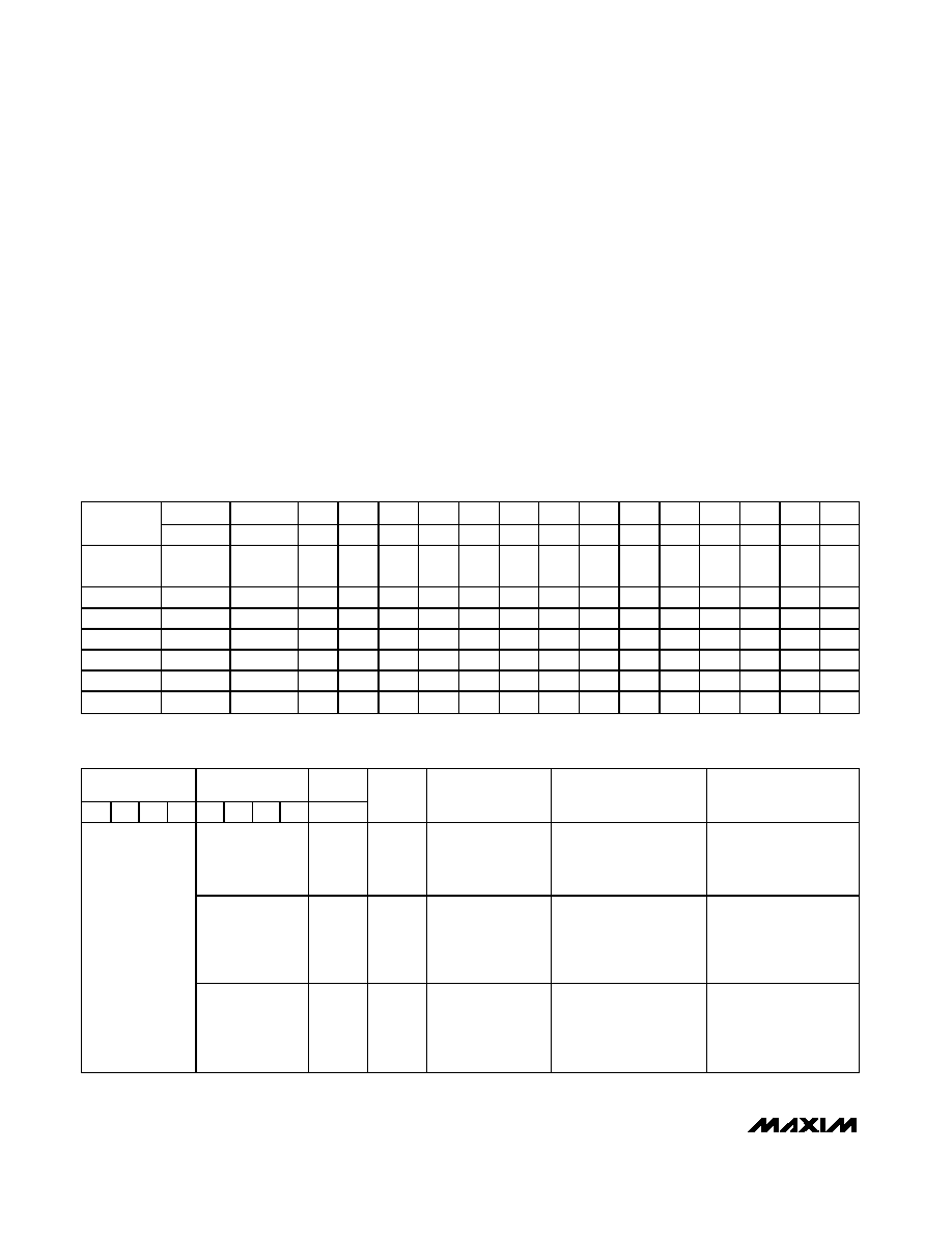
Table 3. MAX19700 Mode Control
D11
D10
D9
D8
D7
D6
D5
D4
D3
D2
D1
D0
A3
A2
A1
A0
REGISTER
NAME
(MSB)
15
14
13
12
11
10
9
8
7
6
5
4
3
2
1
ENABLE-16
E11 = 0
Reserved
E10 = 0
Reserved
—
E7
E6
E5
E4
E3
E2
E1
E0
0
Aux-DAC1
1D11
1D10
1D9
1D8
1D7
1D6
1D5
1D4
1D3
1D2
1D1
1D0
0
1
Aux-DAC2
2D11
2D10
2D9
2D8
2D7
2D6
2D5
2D4
2D3
2D2
2D1
2D0
0
1
0
Aux-DAC3
3D11
3D10
3D9
3D8
3D7
3D6
3D5
3D4
3D3
3D2
3D1
3D0
0
1
IOFFSET
——
—
IO5
IO4
IO3
IO2
IO1
IO0
0
1
0
QOFFSET
——
—
QO5
QO4
QO3
QO2
QO1
QO0
0
1
0
1
COMSEL
——
—
CM1
CM0
0
1
0
Table 4. Power-Management Modes
ADDRESS
DATA BITS
T/
R
A3 A2 A1
A0
E3
E2
E1 E0
PIN 27
MODE
FUNCTION
(POWER
MANAGEMENT)
DESCRIPTION
COMMENT
X000
X
SHDN
SHUTDOWN
Rx ADC = OFF
Tx DAC = OFF
Aux-DAC = OFF
REF = OFF
Device is in complete
shutdown
Overrides T/R pin
X001
X
IDLE
Rx ADC = OFF
Tx DAC = OFF
Aux-DAC = Last State
CLK = ON
REF = ON
Fast turn-on time
Moderate idle power
Overrides T/R pin
0000
X010
X
STBY
STANDBY
Rx ADC = OFF
Tx DAC = OFF
Aux-DAC = Last State
CLK = OFF
REF = ON
Slow turn-on time
Low standby power
Overrides T/R pin
QSPI is a trademark of Motorola, Inc.
X = Don't care.
相关PDF资料 |
PDF描述 |
|---|---|
| MAX5864ETM+ | IC ANLG FRONT END 22MSPS 48-TQFN |
| MAX19711ETN+ | IC ANLG FRONT END 11MSPS 56-TQFN |
| V300C2M50BF3 | CONVERTER MOD DC/DC 2V 50W |
| MAX9140EXK+T | IC COMPARATOR R-R SC70-5 |
| V300C2M50BF | CONVERTER MOD DC/DC 2V 50W |
相关代理商/技术参数 |
参数描述 |
|---|---|
| MAX19700ETM+ | 功能描述:ADC / DAC多通道 7.5Msps CODEC/AFE 1.8/2.7-3.3V RoHS:否 制造商:Texas Instruments 转换速率: 分辨率:8 bit 接口类型:SPI 电压参考: 电源电压-最大:3.6 V 电源电压-最小:2 V 最大工作温度:+ 85 C 安装风格:SMD/SMT 封装 / 箱体:VQFN-40 |
| MAX19700ETM+T | 功能描述:ADC / DAC多通道 7.5Msps CODEC/AFE 1.8/2.7-3.3V RoHS:否 制造商:Texas Instruments 转换速率: 分辨率:8 bit 接口类型:SPI 电压参考: 电源电压-最大:3.6 V 电源电压-最小:2 V 最大工作温度:+ 85 C 安装风格:SMD/SMT 封装 / 箱体:VQFN-40 |
| MAX19700ETM-T | 功能描述:ADC / DAC多通道 RoHS:否 制造商:Texas Instruments 转换速率: 分辨率:8 bit 接口类型:SPI 电压参考: 电源电压-最大:3.6 V 电源电压-最小:2 V 最大工作温度:+ 85 C 安装风格:SMD/SMT 封装 / 箱体:VQFN-40 |
| MAX19700EVCMOD2 | 功能描述:ADC / DAC多通道 Evaluation Kit/Evaluation System for the MAX19700 RoHS:否 制造商:Texas Instruments 转换速率: 分辨率:8 bit 接口类型:SPI 电压参考: 电源电压-最大:3.6 V 电源电压-最小:2 V 最大工作温度:+ 85 C 安装风格:SMD/SMT 封装 / 箱体:VQFN-40 |
| MAX19700EVKIT | 功能描述:数据转换 IC 开发工具 RoHS:否 制造商:Texas Instruments 产品:Demonstration Kits 类型:ADC 工具用于评估:ADS130E08 接口类型:SPI 工作电源电压:- 6 V to + 6 V |
发布紧急采购,3分钟左右您将得到回复。