- 您现在的位置:买卖IC网 > PDF目录10754 > MAX19707ETM+ (Maxim Integrated Products)IC ANLG FRONT END 45MSPS 48-TQFN PDF资料下载
参数资料
| 型号: | MAX19707ETM+ |
| 厂商: | Maxim Integrated Products |
| 文件页数: | 26/37页 |
| 文件大小: | 0K |
| 描述: | IC ANLG FRONT END 45MSPS 48-TQFN |
| 产品培训模块: | Lead (SnPb) Finish for COTS Obsolescence Mitigation Program |
| 标准包装: | 43 |
| 位数: | 10 |
| 通道数: | 4 |
| 功率(瓦特): | 84.6mW |
| 电压 - 电源,模拟: | 3V |
| 电压 - 电源,数字: | 3V |
| 封装/外壳: | 48-WFQFN 裸露焊盘 |
| 供应商设备封装: | 48-TQFN-EP(7x7) |
| 包装: | 管件 |
| 产品目录页面: | 1398 (CN2011-ZH PDF) |
第1页第2页第3页第4页第5页第6页第7页第8页第9页第10页第11页第12页第13页第14页第15页第16页第17页第18页第19页第20页第21页第22页第23页第24页第25页当前第26页第27页第28页第29页第30页第31页第32页第33页第34页第35页第36页第37页
MAX19707
10-Bit, 45Msps, Ultra-Low-Power
Analog Front-End
32
______________________________________________________________________________________
0
2
1
4
3
7
6
5
000
010
001
011
100
101
110
AT STEP
011 (0.5 LSB)
AT STEP
001 (0.25 LSB)
111
DIGITAL INPUT CODE
ANALOG
OUTPUT
VALUE
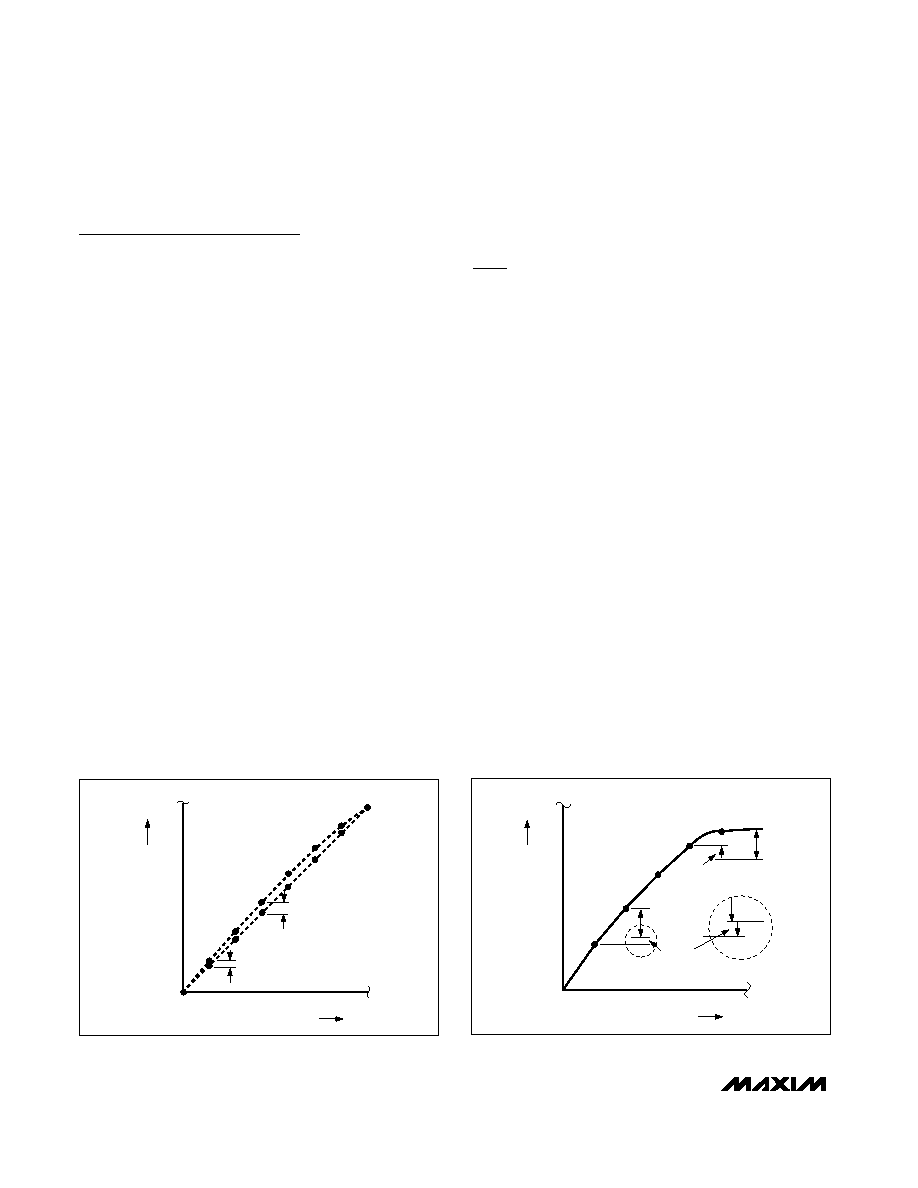
Figure 13a. Integral Nonlinearity
0
2
1
4
3
6
5
000
010
001
011
100
101
DIFFERENTIAL LINEARITY
ERROR (-0.25 LSB)
DIFFERENTIAL
LINEARITY ERROR (+0.25 LSB)
1 LSB
DIGITAL INPUT CODE
ANALOG
OUTPUT
VALUE
Figure 13b. Differential Nonlinearity
Grounding, Bypassing, and
Board Layout
The MAX19707 requires high-speed board layout
design techniques. Refer to the MAX19707 EV kit data
sheet for a board layout reference. Place all bypass
capacitors as close to the device as possible, prefer-
ably on the same side of the board as the device, using
surface-mount devices for minimum inductance.
Bypass VDD to GND with a 0.1F ceramic capacitor in
parallel with a 2.2F capacitor. Bypass OVDD to OGND
with a 0.1F ceramic capacitor in parallel with a 2.2F
capacitor. Bypass REFP, REFN, and COM each to
GND with a 0.33F ceramic capacitor. Bypass REFIN
to GND with a 0.1F capacitor.
Multilayer boards with separated ground and power
planes yield the highest level of signal integrity. Use a
split ground plane arranged to match the physical loca-
tion of the analog ground (GND) and the digital output-
driver ground (OGND) on the device package.
Connect the MAX19707 exposed backside paddle to
GND plane. Join the two ground planes at a single
point so the noisy digital ground currents do not inter-
fere with the analog ground plane. The ideal location
for this connection can be determined experimentally
at a point along the gap between the two ground
planes. Make this connection with a low-value, surface-
mount resistor (1
Ω to 5Ω), a ferrite bead, or a direct
short. Alternatively, all ground pins could share the
same ground plane, if the ground plane is sufficiently
isolated from any noisy digital system’s ground plane
(e.g., downstream output buffer or DSP ground plane).
Route high-speed digital signal traces away from sensi-
tive analog traces. Make sure to isolate the analog
input lines to each respective converter to minimize
channel-to-channel crosstalk. Keep all signal lines
short and free of 90° turns.
Dynamic Parameter Definitions
ADC and DAC Static Parameter Definitions
Integral Nonlinearity (INL)
Integral nonlinearity is the deviation of the values on an
actual transfer function from a straight line. This straight
line can be either a best-straight-line fit or a line drawn
between the end points of the transfer function, once
offset and gain errors have been nullified. The static lin-
earity parameters for the device are measured using
the best-straight-line fit (DAC Figure 13a).
Differential Nonlinearity (DNL)
Differential nonlinearity is the difference between an
actual step width and the ideal value of 1 LSB. A DNL
error specification of less than 1 LSB guarantees no
missing codes (ADC) and a monotonic transfer function
(ADC and DAC) (DAC Figure 13b).
ADC Offset Error
Ideally, the midscale transition occurs at 0.5 LSB above
midscale. The offset error is the amount of deviation
between the measured transition point and the ideal
transition point.
DAC Offset Error
Offset error (Figure 13a) is the difference between the
ideal and actual offset point. The offset point is the out-
put value when the digital input is midscale. This error
affects all codes by the same amount and usually can
be compensated by trimming.
相关PDF资料 |
PDF描述 |
|---|---|
| MAX5865ETM+ | IC ANLG FRONT END 40MSPS 48-TQFN |
| VE-J3P-MY-F4 | CONVERTER MOD DC/DC 13.8V 50W |
| 73M1903-IM/F | IC MODEM AFE V.22BIS 32-QFN |
| VE-J3P-MY-F3 | CONVERTER MOD DC/DC 13.8V 50W |
| ISL51002CQZ-165 | IC FRONT END 10BIT VID 128-MQFP |
相关代理商/技术参数 |
参数描述 |
|---|---|
| MAX19707ETM+ | 功能描述:ADC / DAC多通道 45Msps CODEC/AFE 1.8/2.7-3.3V RoHS:否 制造商:Texas Instruments 转换速率: 分辨率:8 bit 接口类型:SPI 电压参考: 电源电压-最大:3.6 V 电源电压-最小:2 V 最大工作温度:+ 85 C 安装风格:SMD/SMT 封装 / 箱体:VQFN-40 |
| MAX19707ETM+T | 功能描述:ADC / DAC多通道 45Msps CODEC/AFE 1.8/2.7-3.3V RoHS:否 制造商:Texas Instruments 转换速率: 分辨率:8 bit 接口类型:SPI 电压参考: 电源电压-最大:3.6 V 电源电压-最小:2 V 最大工作温度:+ 85 C 安装风格:SMD/SMT 封装 / 箱体:VQFN-40 |
| MAX19707ETM-T | 功能描述:ADC / DAC多通道 RoHS:否 制造商:Texas Instruments 转换速率: 分辨率:8 bit 接口类型:SPI 电压参考: 电源电压-最大:3.6 V 电源电压-最小:2 V 最大工作温度:+ 85 C 安装风格:SMD/SMT 封装 / 箱体:VQFN-40 |
| MAX19707EVCMOD2 | 功能描述:ADC / DAC多通道 Evaluation System for the MAX19707 RoHS:否 制造商:Texas Instruments 转换速率: 分辨率:8 bit 接口类型:SPI 电压参考: 电源电压-最大:3.6 V 电源电压-最小:2 V 最大工作温度:+ 85 C 安装风格:SMD/SMT 封装 / 箱体:VQFN-40 |
| MAX19707EVCMODU | 功能描述:ADC / DAC多通道 Evaluation System for the MAX19707 RoHS:否 制造商:Texas Instruments 转换速率: 分辨率:8 bit 接口类型:SPI 电压参考: 电源电压-最大:3.6 V 电源电压-最小:2 V 最大工作温度:+ 85 C 安装风格:SMD/SMT 封装 / 箱体:VQFN-40 |
发布紧急采购,3分钟左右您将得到回复。