- 您现在的位置:买卖IC网 > PDF目录10754 > MAX19707ETM+ (Maxim Integrated Products)IC ANLG FRONT END 45MSPS 48-TQFN PDF资料下载
参数资料
| 型号: | MAX19707ETM+ |
| 厂商: | Maxim Integrated Products |
| 文件页数: | 9/37页 |
| 文件大小: | 0K |
| 描述: | IC ANLG FRONT END 45MSPS 48-TQFN |
| 产品培训模块: | Lead (SnPb) Finish for COTS Obsolescence Mitigation Program |
| 标准包装: | 43 |
| 位数: | 10 |
| 通道数: | 4 |
| 功率(瓦特): | 84.6mW |
| 电压 - 电源,模拟: | 3V |
| 电压 - 电源,数字: | 3V |
| 封装/外壳: | 48-WFQFN 裸露焊盘 |
| 供应商设备封装: | 48-TQFN-EP(7x7) |
| 包装: | 管件 |
| 产品目录页面: | 1398 (CN2011-ZH PDF) |
第1页第2页第3页第4页第5页第6页第7页第8页当前第9页第10页第11页第12页第13页第14页第15页第16页第17页第18页第19页第20页第21页第22页第23页第24页第25页第26页第27页第28页第29页第30页第31页第32页第33页第34页第35页第36页第37页
MAX19707
10-Bit, 45Msps, Ultra-Low-Power
Analog Front-End
______________________________________________________________________________________
17
Rx ADC System Timing Requirements
Figure 3 shows the relationship between the clock, ana-
log inputs, and the resulting output data. Channel I
(CHI) and channel Q (CHQ) are sampled on the rising
edge of the clock signal (CLK) and the resulting data is
multiplexed at the D0–D9 outputs. CHI data is updated
on the rising edge and CHQ data is updated on the
falling edge of the CLK. Including the delay through the
output latch, the total clock-cycle latency is 5 clock
cycles for CHI and 5.5 clock cycles for CHQ.
Digital Input/Output Data (D0–D9)
D0–D9 are the Rx ADC digital logic outputs when the
MAX19707 is in receive mode. This bus is shared with
the Tx DAC digital logic inputs and operates in half-
duplex mode. D0–D9 are the Tx DAC digital logic inputs
when the MAX19707 is in transmit mode. The logic level
is set by OVDD from 1.8V to VDD. The digital output cod-
ing is offset binary (Table 1). Keep the capacitive load
on the digital outputs D0–D9 as low as possible (< 15pF)
to avoid large digital currents feeding back into the ana-
log portion of the MAX19707 and degrading its dynamic
performance. Buffers on the digital outputs isolate the out-
puts from heavy capacitive loads. Adding 100
Ω resistors
in series with the digital outputs close to the MAX19707
helps improve Rx ADC and Tx DAC performance. Refer
to the MAX19707EVKIT schematic for an example of the
digital outputs driving a digital buffer through 100
Ω series
resistors.
During SHDN, IDLE, and STBY states, D0–D9 are inter-
nally pulled up to prevent floating digital inputs. To ensure
no current flows through D0–D9 I/O, the external bus
needs to be either tri-stated or pulled up to OVDD and
should not be pulled to ground.
Table 1. Rx ADC Output Codes vs. Input Voltage
DIFFERENTIAL INPUT
VOLTAGE
DIFFERENTIAL INPUT (LSB)
OFFSET BINARY (D0–D9)
OUTPUT DECIMAL CODE
VREF x 512/512
511 (+Full Scale - 1 LSB)
11 1111 1111
1023
VREF x 511/512
510 (+Full Scale - 2 LSB)
11 1111 1110
1022
VREF x 1/512
+1
10 0000 0001
513
VREF x 0/512
0 (Bipolar Zero)
10 0000 0000
512
-VREF x 1/512
-1
01 1111 1111
511
-VREF x 511/512
-511 (-Full Scale +1 LSB)
00 0000 0001
1
-VREF x 512/512
-512 (-Full Scale)
00 0000 0000
0
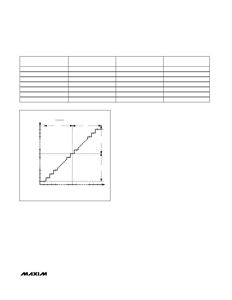
Figure 2. Rx ADC Transfer Function
INPUT VOLTAGE (LSB)
-1
-510 -509
1024
2 x VREF
1 LSB =
VREF = VREFP - VREFN
VREF
V
REF
V
REF
0+ 1
-511
+510
+512
+511
-512
+509
(COM)
OFFSET
BINAR
Y
OUTPUT
CODE
(LSB)
00 0000 0000
00 0000 0001
00 0000 0010
00 0000 0011
11 1111 1111
11 1111 1110
11 1111 1101
01 1111 1111
10 0000 0000
10 0000 0001
相关PDF资料 |
PDF描述 |
|---|---|
| MAX5865ETM+ | IC ANLG FRONT END 40MSPS 48-TQFN |
| VE-J3P-MY-F4 | CONVERTER MOD DC/DC 13.8V 50W |
| 73M1903-IM/F | IC MODEM AFE V.22BIS 32-QFN |
| VE-J3P-MY-F3 | CONVERTER MOD DC/DC 13.8V 50W |
| ISL51002CQZ-165 | IC FRONT END 10BIT VID 128-MQFP |
相关代理商/技术参数 |
参数描述 |
|---|---|
| MAX19707ETM+ | 功能描述:ADC / DAC多通道 45Msps CODEC/AFE 1.8/2.7-3.3V RoHS:否 制造商:Texas Instruments 转换速率: 分辨率:8 bit 接口类型:SPI 电压参考: 电源电压-最大:3.6 V 电源电压-最小:2 V 最大工作温度:+ 85 C 安装风格:SMD/SMT 封装 / 箱体:VQFN-40 |
| MAX19707ETM+T | 功能描述:ADC / DAC多通道 45Msps CODEC/AFE 1.8/2.7-3.3V RoHS:否 制造商:Texas Instruments 转换速率: 分辨率:8 bit 接口类型:SPI 电压参考: 电源电压-最大:3.6 V 电源电压-最小:2 V 最大工作温度:+ 85 C 安装风格:SMD/SMT 封装 / 箱体:VQFN-40 |
| MAX19707ETM-T | 功能描述:ADC / DAC多通道 RoHS:否 制造商:Texas Instruments 转换速率: 分辨率:8 bit 接口类型:SPI 电压参考: 电源电压-最大:3.6 V 电源电压-最小:2 V 最大工作温度:+ 85 C 安装风格:SMD/SMT 封装 / 箱体:VQFN-40 |
| MAX19707EVCMOD2 | 功能描述:ADC / DAC多通道 Evaluation System for the MAX19707 RoHS:否 制造商:Texas Instruments 转换速率: 分辨率:8 bit 接口类型:SPI 电压参考: 电源电压-最大:3.6 V 电源电压-最小:2 V 最大工作温度:+ 85 C 安装风格:SMD/SMT 封装 / 箱体:VQFN-40 |
| MAX19707EVCMODU | 功能描述:ADC / DAC多通道 Evaluation System for the MAX19707 RoHS:否 制造商:Texas Instruments 转换速率: 分辨率:8 bit 接口类型:SPI 电压参考: 电源电压-最大:3.6 V 电源电压-最小:2 V 最大工作温度:+ 85 C 安装风格:SMD/SMT 封装 / 箱体:VQFN-40 |
发布紧急采购,3分钟左右您将得到回复。