- 您现在的位置:买卖IC网 > PDF目录10753 > MAX19710ETN+ (Maxim Integrated Products)IC ANLG FRONT END 7.5MSPS 56TQFN PDF资料下载
参数资料
| 型号: | MAX19710ETN+ |
| 厂商: | Maxim Integrated Products |
| 文件页数: | 8/37页 |
| 文件大小: | 0K |
| 描述: | IC ANLG FRONT END 7.5MSPS 56TQFN |
| 产品变化通告: | Product Discontinuation 09/Jun/2011 |
| 标准包装: | 43 |
| 位数: | 10 |
| 通道数: | 2 |
| 功率(瓦特): | 30mW |
| 电压 - 电源,模拟: | 3V |
| 电压 - 电源,数字: | 3V |
| 封装/外壳: | 56-WFQFN 裸露焊盘 |
| 供应商设备封装: | 56-TQFN-EP(7x7) |
| 包装: | 管件 |
| 产品目录页面: | 1398 (CN2011-ZH PDF) |
第1页第2页第3页第4页第5页第6页第7页当前第8页第9页第10页第11页第12页第13页第14页第15页第16页第17页第18页第19页第20页第21页第22页第23页第24页第25页第26页第27页第28页第29页第30页第31页第32页第33页第34页第35页第36页第37页
MAX19710
10-Bit, 7.5Msps, Full-Duplex
Analog Front-End
16
______________________________________________________________________________________
16
______________________________________________________________________________________
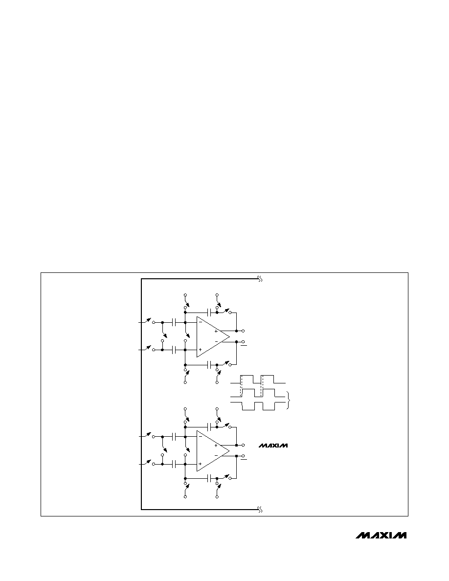
Figure 1. Rx ADC Internal T/H Circuits
The MAX19710 integrates three 12-bit auxiliary DACs
(aux-DACs) and a 10-bit, 333ksps auxiliary ADC (aux-
ADC) with 4:1 input multiplexer. The aux-DAC channels
feature 1s settling time for fast AGC, VGA, and AFC
level setting. The aux-ADC features data averaging to
reduce processor overhead and a selectable clock-
divider to program the conversion rate.
The MAX19710 includes a 3-wire serial interface to con-
trol operating modes and power management. The seri-
al interface is SPI and MICROWIRE compatible.
The MAX19710 serial interface selects shutdown, idle,
standby, FD, transmit (Tx), and receive (Rx) modes, as
well as controls aux-DAC and aux-ADC channels.
The MAX19710 features two independent, high-speed,
10-bit buses for the Rx ADC and Tx DAC, which allow
full-duplex (FD) operation for frequency-division duplex
applications. Each bus can be disabled to optimize
power management through the 3-wire interface. The
MAX19710 operates from a single 2.7V to 3.3V analog
supply and a 1.8V to 3.3V digital supply.
Dual 10-Bit Rx ADC
The ADC uses a seven-stage, fully differential, pipelined
architecture that allows for high-speed conversion while
minimizing power consumption. Samples taken at the
inputs move progressively through the pipeline stages
every half clock cycle. Including the delay through the
output latch, the total clock-cycle latency is 5 clock
cycles for channel IA and 5.5 clock cycles for channel
QA. The ADC full-scale analog input range is ±VREF
with a VDD / 2 (±0.8V) common-mode input range. VREF
is the difference between VREFP and VREFN. See the
Reference Configurations section for details.
Input Track-and-Hold (T/H) Circuits
Figure 1 displays a simplified diagram of the Rx ADC
input track-and-hold (T/H) circuitry. Both ADC inputs
(IAP, QAP, IAN, and QAN) can be driven either differen-
S3b
S3a
COM
S5b
S5a
QAP
QAN
S1
OUT
C2a
C2b
S4c
S4a
S4b
C1b
C1a
INTERNAL
BIAS
INTERNAL
BIAS
COM
HOLD
CLK
INTERNAL
NONOVERLAPPING
CLOCK SIGNALS
TRACK
S2a
S2b
S3b
S3a
COM
S5b
S5a
IAP
IAN
S1
OUT
C2a
C2b
S4c
S4a
S4b
C1b
C1a
INTERNAL
BIAS
INTERNAL
BIAS
COM
S2a
S2b
MAX19710
MICROWIRE is a trademark of National Semiconductor Corp.
SPI is a trademark of Motorola, Inc.
相关PDF资料 |
PDF描述 |
|---|---|
| V300C2M50BG2 | CONVERTER MOD DC/DC 2V 50W |
| MAX19713ETN+ | IC ANLG FRONT END 45MSPS 56-TQFN |
| MAX9061EUK+T | IC COMPARATOR SGL LP SOT23-5 |
| V300C2M50BG | CONVERTER MOD DC/DC 2V 50W |
| MAX19700ETM+ | IC ANLG FRONT END 7.5MSPS 48TQFN |
相关代理商/技术参数 |
参数描述 |
|---|---|
| MAX19710ETN+ | 功能描述:ADC / DAC多通道 7.5Msps CODEC/AFE Full Duplex RoHS:否 制造商:Texas Instruments 转换速率: 分辨率:8 bit 接口类型:SPI 电压参考: 电源电压-最大:3.6 V 电源电压-最小:2 V 最大工作温度:+ 85 C 安装风格:SMD/SMT 封装 / 箱体:VQFN-40 |
| MAX19710ETN+T | 功能描述:ADC / DAC多通道 7.5Msps CODEC/AFE Full Duplex RoHS:否 制造商:Texas Instruments 转换速率: 分辨率:8 bit 接口类型:SPI 电压参考: 电源电压-最大:3.6 V 电源电压-最小:2 V 最大工作温度:+ 85 C 安装风格:SMD/SMT 封装 / 箱体:VQFN-40 |
| MAX19710ETN-T | 功能描述:ADC / DAC多通道 RoHS:否 制造商:Texas Instruments 转换速率: 分辨率:8 bit 接口类型:SPI 电压参考: 电源电压-最大:3.6 V 电源电压-最小:2 V 最大工作温度:+ 85 C 安装风格:SMD/SMT 封装 / 箱体:VQFN-40 |
| MAX19710EVCMODU+ | 功能描述:数据转换 IC 开发工具 MAX19710 Eval System RoHS:否 制造商:Texas Instruments 产品:Demonstration Kits 类型:ADC 工具用于评估:ADS130E08 接口类型:SPI 工作电源电压:- 6 V to + 6 V |
| MAX19710EVKIT | 功能描述:数据转换 IC 开发工具 RoHS:否 制造商:Texas Instruments 产品:Demonstration Kits 类型:ADC 工具用于评估:ADS130E08 接口类型:SPI 工作电源电压:- 6 V to + 6 V |
发布紧急采购,3分钟左右您将得到回复。