- 您现在的位置:买卖IC网 > PDF目录13119 > MAX1997ETJ+ (Maxim Integrated Products)IC PWR SUPPLY TFT LCD 32TQFN PDF资料下载
参数资料
| 型号: | MAX1997ETJ+ |
| 厂商: | Maxim Integrated Products |
| 文件页数: | 12/31页 |
| 文件大小: | 0K |
| 描述: | IC PWR SUPPLY TFT LCD 32TQFN |
| 产品培训模块: | Lead (SnPb) Finish for COTS Obsolescence Mitigation Program |
| 标准包装: | 60 |
| 应用: | 控制器,TFT LCD |
| 输入电压: | 2.7 V ~ 5.5 V |
| 输出数: | 5 |
| 输出电压: | 2.7 V ~ 13 V |
| 工作温度: | 0°C ~ 85°C |
| 安装类型: | 表面贴装 |
| 封装/外壳: | 32-WFQFN 裸露焊盘 |
| 供应商设备封装: | 32-TQFN-EP(5x5) |
| 包装: | 管件 |
第1页第2页第3页第4页第5页第6页第7页第8页第9页第10页第11页当前第12页第13页第14页第15页第16页第17页第18页第19页第20页第21页第22页第23页第24页第25页第26页第27页第28页第29页第30页第31页
�� �
�
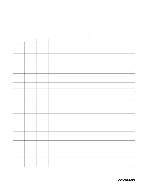
�Quintuple/Triple-Output� TFT� LCD� Power� Supplies�
�with� Fault� Protection� and� VCOM� Buffer�
�Pin� Description� (continued)�
�PIN�
�MAX1997� MAX1998�
�NAME�
�FUNCTION�
�Gamma� Linear-Regulator� (REG� 2)� Base� Drive.� Open� drain� of� an� internal� N-channel� MOSFET.�
�19�
�—�
�DRV2�
�Connect� DRV2� to� the� base� of� an� external� PNP� linear� regulator� pass� transistor.� (See� the� Pass�
�Transistor� Selection� section.)�
�Main� Step-Up� Regulator� Feedback� Input.� Connect� FB� to� the� center� tap� of� a� resistive� voltage-�
�20�
�11�
�FB�
�divider� between� the� main� output� (V� MAIN� )� and� the� analog� ground� (GND)� to� set� the� main� step-�
�up� regulator� output� voltage.� (See� the� Main� Step-Up� Regulator,� Output� Voltage� Selection�
�section.)� Place� the� resistive� voltage-divider� close� to� the� pin.�
�Gate-On� Linear-Regulator� (REG� P)� Feedback� Input.� FBP� regulates� to� 1.25V� nominal.� Connect�
�21�
�12�
�FBP�
�FBP� to� the� center� tap� of� a� resistive� voltage-divider� between� the� REG� P� output� and� the� analog�
�ground� (GND)� to� set� the� output� voltage.� Place� the� resistive� voltage-divider� close� to� the� pin.�
�Gate-On� Linear-Regulator� (REG� P)� Base� Drive.� Open� drain� of� an� internal� N-channel� MOSFET.�
�22�
�13�
�DRVP�
�Connect� DRVP� to� the� base� of� an� external� PNP� linear-regulator� pass� transistor.� (See� the� Pass�
�Transistor� Selection� section.)�
�23�
�24�
�14�
�15�
�LX�
�TGNDA�
�Switching� Node.� Drain� of� the� internal� N-channel� power� MOSFET� for� the� main� step-up�
�regulator.�
�Internal� Connection.� Connect� this� pin� to� ground.� Do� not� leave� this� pin� floating.�
�Overcurrent� Comparator� Inverting� Input.� Connect� OCN� to� the� center� tap� of� a� resistive�
�25�
�16�
�OCN�
�voltage-divider� connected� to� the� drain� of� the� external� input� protection� P-channel� MOSFET.�
�(See� the� Input� Overcurrent� Protection� section.)� If� unused,� connect� OCN� to� REF.�
�Overcurrent� Comparator� Noninverting� Input.� Connect� OCP� to� the� center� tap� of� a� resistive�
�26�
�17�
�OCP�
�voltage-divider� connected� to� the� source� of� the� external� input� protection� P-channel� MOSFET.�
�The� voltage� on� OCP� sets� the� input� overcurrent� threshold.� (See� the� Input� Overcurrent�
�Protection� section.)� If� unused,� connect� OCP� to� GND.�
�27�
�18�
�GATE�
�Gate-Drive� Output� to� the� External� Input� Protection� P-Channel� MOSFET.� (See� the� Input�
�Overcurrent� Protection� section.)� If� unused,� leave� GATE� unconnected.�
�Fault� Timer� Select� Input.� Pull� PFLT� above� its� logic� high� threshold� (0.7� � V� IN� )� to� set� the� fault�
�28�
�—�
�PFLT�
�delay� period� to� 87ms.� Pull� PFLT� below� its� logic� low� threshold� (0.3� � V� IN� )� to� set� the� fault� delay�
�period� to� 22ms.� Leave� PFLT� unconnected� to� set� the� fault� delay� period� to� 44ms.� The� fault�
�delay� period� for� the� MAX1998� is� fixed� at� 87ms.�
�Supply� Input.� The� supply� voltage� powers� all� the� control� circuitry.� The� input� voltage� range� is�
�29�
�19�
�IN�
�from� 2.7V� to� 5.5V.� Bypass� IN� to� GND� with� a� 0.47μF� ceramic� capacitor.� Place� the� capacitor�
�within� 5mm� of� IN.�
�30�
�—�
�ONDC�
�Step-Up� Regulator� Logic� Control� Input.� The� step-up� regulator,� VCOM� buffer,� and� the� sequence�
�timing� block� are� enabled� when� ONDC� is� high� and� disabled� when� ONDC� is� low.�
�Frequency� Select� Input.� Pull� FREQ� above� its� logic� high� threshold� (0.7� � V� IN� )� to� set� the� main�
�31�
�20�
�FREQ�
�step-up� regulator� switching� frequency� to� 1.5MHz.� Pull� FREQ� below� its� logic� low� threshold�
�(0.3� � V� IN� )� to� set� the� frequency� to� 375kHz.� Leave� FREQ� unconnected� to� set� the� frequency�
�to� 750kHz.�
�Active-Low� Shutdown� Control� Input.� All� the� sections� of� the� device� are� disabled� and� the� GATE�
�32�
�—�
�SHDN�
�pin� goes� high� when� SHDN� is� below� its� 0.4V� logic� low� threshold.� Pull� SHDN� above� its� 1.6V�
�logic� high� threshold� to� enable� the� device.� Do� not� leave� SHDN� unconnected.�
�12�
�______________________________________________________________________________________�
�相关PDF资料 |
PDF描述 |
|---|---|
| EBM28DTMT-S189 | CONN EDGECARD 56POS R/A .156 SLD |
| ABM15DSES-S243 | CONN EDGECARD 30POS .156 EYELET |
| VI-J6V-CX | CONVERTER MOD DC/DC 5.8V 75W |
| VE-2WB-EW-B1 | CONVERTER MOD DC/DC 95V 100W |
| GBM31DTMT-S189 | CONN EDGECARD 62POS R/A .156 SLD |
相关代理商/技术参数 |
参数描述 |
|---|---|
| MAX1997ETJ+ | 功能描述:其他电源管理 Quint/Triple-Out TFT LCD Power Supply RoHS:否 制造商:Texas Instruments 输出电压范围: 输出电流:4 mA 输入电压范围:3 V to 3.6 V 输入电流: 功率耗散: 工作温度范围:- 40 C to + 110 C 安装风格:SMD/SMT 封装 / 箱体:VQFN-48 封装:Reel |
| MAX1997ETJ+T | 功能描述:LCD 驱动器 Quint/Triple-Out TFT LCD Power Supply RoHS:否 制造商:Maxim Integrated 数位数量:4.5 片段数量:30 最大时钟频率:19 KHz 工作电源电压:3 V to 3.6 V 最大工作温度:+ 85 C 最小工作温度:- 20 C 封装 / 箱体:PDIP-40 封装:Tube |
| MAX1997ETJ-T | 功能描述:其他电源管理 RoHS:否 制造商:Texas Instruments 输出电压范围: 输出电流:4 mA 输入电压范围:3 V to 3.6 V 输入电流: 功率耗散: 工作温度范围:- 40 C to + 110 C 安装风格:SMD/SMT 封装 / 箱体:VQFN-48 封装:Reel |
| MAX1997EVKIT | 制造商:Maxim Integrated Products 功能描述:QUINTUPLE/TRIPLE OUTPUT TFT LCD POWER SUPPLIE - Bulk |
| MAX19983A | 功能描述:上下转换器 RoHS:否 制造商:Texas Instruments 产品:Down Converters 射频:52 MHz to 78 MHz 中频:300 MHz LO频率: 功率增益: P1dB: 工作电源电压:1.8 V, 3.3 V 工作电源电流:120 mA 最大功率耗散:1 W 最大工作温度:+ 85 C 安装风格:SMD/SMT 封装 / 箱体:PQFP-128 |
发布紧急采购,3分钟左右您将得到回复。