- 您现在的位置:买卖IC网 > Datasheet目录472 > MAX2120EVKIT+ (Maxim Integrated)KIT EVAL FOR MAX2120 Datasheet资料下载
参数资料
| 型号: | MAX2120EVKIT+ |
| 厂商: | Maxim Integrated |
| 文件页数: | 15/21页 |
| 文件大小: | 0K |
| 描述: | KIT EVAL FOR MAX2120 |
| 产品培训模块: | Lead (SnPb) Finish for COTS Obsolescence Mitigation Program |
| 标准包装: | 1 |
| 类型: | 调谐器 |
| 频率: | 925MHz ~ 2.175GHz |
| 适用于相关产品: | MAX2120 |
| 已供物品: | 板 |
�� �
�
�Complete,� Direct-Conversion� Tuner� for� DVB-S�
�and� Free-to-Air� Applications�
�2-Wire� Serial� Interface�
�The� MAX2120� uses� a� 2-wire� I� 2� C-compatible� serial�
�interface� consisting� of� a� serial� data� line� (SDA)� and� a�
�serial� clock� line� (SCL).� SDA� and� SCL� facilitate� bidirec-�
�tional� communication� between� the� MAX2120� and� the�
�master� at� clock� frequencies� up� to� 400kHz.� The� master�
�initiates� a� data� transfer� on� the� bus� and� generates� the�
�SCL� signal� to� permit� data� transfer.� The� MAX2120�
�behaves� as� a� slave� device� that� transfers� and� receives�
�data� to� and� from� the� master.� SDA� and� SCL� must� be�
�pulled� high� with� external� pullup� resistors� (1k� ?� or�
�greater)� for� proper� bus� operation.�
�One� bit� is� transferred� during� each� SCL� clock� cycle.� A�
�minimum� of� nine� clock� cycles� is� required� to� transfer� a�
�byte� in� or� out� of� the� MAX2120� (8� bits� and� an�
�ACK/NACK).� The� data� on� SDA� must� remain� stable�
�during� the� high� period� of� the� SCL� clock� pulse.� Changes�
�in� SDA� while� SCL� is� high� and� stable� are� considered�
�Slave� Address�
�The� MAX2120� has� a� 7-bit� slave� address� that� must� be�
�sent� to� the� device� following� a� START� condition� to� initi-�
�ate� communication.� The� slave� address� is� internally� pro-�
�grammed� to� 1100000.� The� eighth� bit� (R/� W� )� following�
�the� 7-bit� address� determines� whether� a� read� or� write�
�operation� will� occur.�
�The� MAX2120� continuously� awaits� a� START� condition�
�followed� by� its� slave� address.� When� the� device� recog-�
�nizes� its� slave� address,� it� acknowledges� by� pulling� the�
�SDA� line� low� for� one� clock� period;� it� is� ready� to� accept�
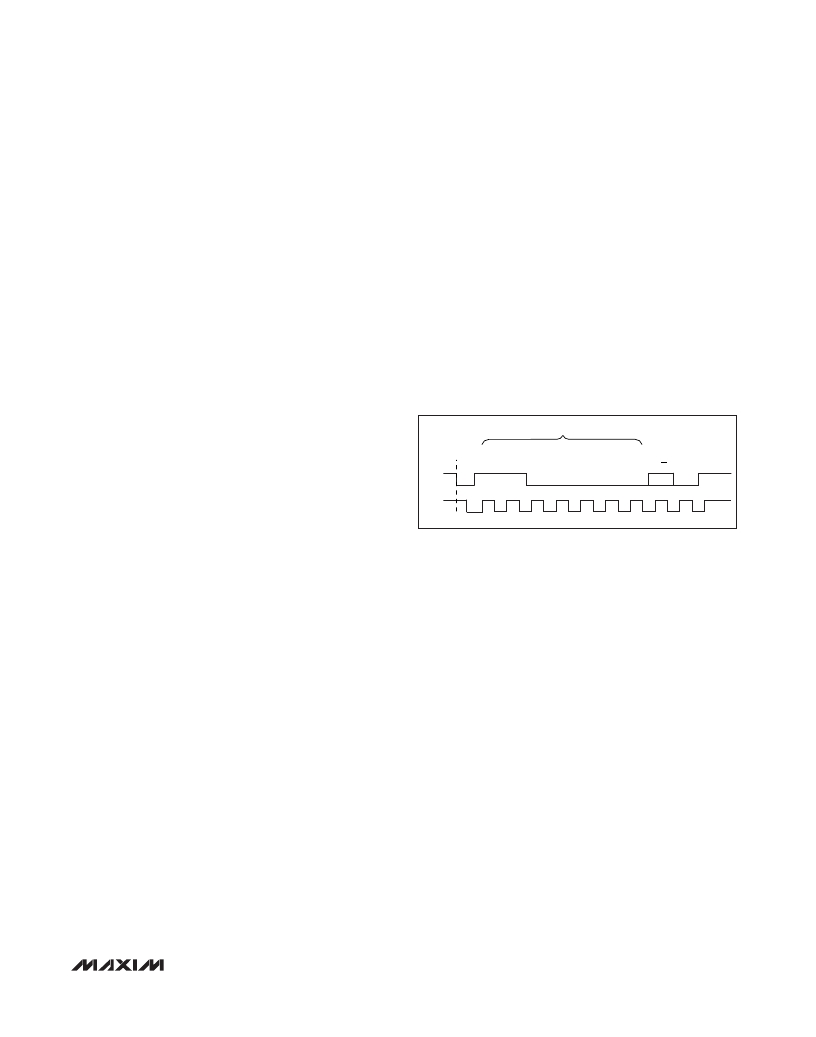
�or� send� data� depending� on� the� R/� W� bit� (Figure� 1).�
�The� write/read� address� is� C0/C1� if� the� ADDR� pin� is� con-�
�nected� to� ground.� The� write/read� address� is� C2/C3� if�
�the� ADDR� pin� is� connected� to� V� CC� .�
�SLAVE� ADDRESS�
�control� signals� (see� the� START� and� STOP� Conditions�
�section).� Both� SDA� and� SCL� remain� high� when� the� bus�
�is� not� busy.� Pullup� resistors� should� be� referenced� to� the�
�SDA�
�S�
�1�
�1�
�0�
�0�
�0�
�0�
�0�
�R/W�
�ACK�
�MAX2120’s� V� CC� .�
�START� and� STOP� Conditions�
�SCL�
�1�
�2�
�3�
�4�
�5�
�6�
�7�
�8�
�9�
�The� master� initiates� a� transmission� with� a� START� condi-�
�tion� (S),� which� is� a� high-to-low� transition� on� SDA� while�
�SCL� is� high.� The� master� terminates� a� transmission� with�
�a� STOP� condition� (P),� which� is� a� low-to-high� transition�
�on� SDA� while� SCL� is� high.�
�Acknowledge� and� Not-Acknowledge� Conditions�
�Data� transfers� are� framed� with� an� acknowledge� bit�
�(ACK)� or� a� not-acknowledge� bit� (NACK).� Both� the� mas-�
�ter� and� the� MAX2120� (slave)� generate� acknowledge�
�bits.� To� generate� an� acknowledge,� the� receiving� device�
�must� pull� SDA� low� before� the� rising� edge� of� the�
�acknowledge-related� clock� pulse� (ninth� pulse)� and�
�keep� it� low� during� the� high� period� of� the� clock� pulse.�
�To� generate� a� not-acknowledge� condition,� the� receiver�
�allows� SDA� to� be� pulled� high� before� the� rising� edge� of�
�the� acknowledge-related� clock� pulse,� and� leaves� SDA�
�high� during� the� high� period� of� the� clock� pulse.�
�Monitoring� the� acknowledge� bits� allows� for� detection� of�
�unsuccessful� data� transfers.� An� unsuccessful� data�
�transfer� happens� if� a� receiving� device� is� busy� or� if� a�
�system� fault� has� occurred.� In� the� event� of� an� unsuc-�
�cessful� data� transfer,� the� bus� master� must� reattempt�
�communication� at� a� later� time.�
�Figure� 1.� MAX2120� Slave� Address� Byte� with� ADDR� Pin�
�Connected� to� Ground�
�Write� Cycle�
�When� addressed� with� a� write� command,� the� MAX2120�
�allows� the� master� to� write� to� a� single� register� or� to� multi-�
�ple� successive� registers.�
�A� write� cycle� begins� with� the� bus� master� issuing� a�
�START� condition� followed� by� the� seven� slave� address�
�bits� and� a� write� bit� (R/� W� =� 0).� The� MAX2120� issues� an�
�ACK� if� the� slave� address� byte� is� successfully� received.�
�The� bus� master� must� then� send� to� the� slave� the�
�address� of� the� first� register� it� wishes� to� write� to� (see�
�Table� 1� for� register� addresses).� If� the� slave� acknowl-�
�edges� the� address,� the� master� can� then� write� one� byte�
�to� the� register� at� the� specified� address.� Data� is� written�
�beginning� with� the� most� significant� bit.� The� MAX2120�
�again� issues� an� ACK� if� the� data� is� successfully� written�
�to� the� register.� The� master� can� continue� to� write� data� to�
�the� successive� internal� registers� with� the� MAX2120�
�acknowledging� each� successful� transfer,� or� it� can� ter-�
�minate� transmission� by� issuing� a� STOP� condition.� The�
�write� cycle� will� not� terminate� until� the� master� issues� a�
�STOP� condition.�
�______________________________________________________________________________________�
�15�
�相关PDF资料 |
PDF描述 |
|---|---|
| MAX2121EVKIT# | KIT EVAL FOR MAX2121 |
| MAX2130EVKIT | EVAL KIT MAX2130 |
| MAX2140EVKIT | EVAL KIT MAX2140 |
| MAX2150ETI+T | IC MODULATOR I/Q WIDE 28TQFN |
| MAX2160EVKIT | EVAL KIT MAX2160 |
相关代理商/技术参数 |
参数描述 |
|---|---|
| MAX2120EVKIT+ | 功能描述:射频开发工具 MAX2120 Eval Kit RoHS:否 制造商:Taiyo Yuden 产品:Wireless Modules 类型:Wireless Audio 工具用于评估:WYSAAVDX7 频率: 工作电源电压:3.4 V to 5.5 V |
| MAX2121 | 制造商:MAXIM 制造商全称:Maxim Integrated Products 功能描述:Complete Direct-Conversion L-Band Tuner |
| MAX2121_V1 | 制造商:MAXIM 制造商全称:Maxim Integrated Products 功能描述:Complete Direct-Conversion L-Band Tuner |
| MAX2121ETI | 制造商:MAXIM 制造商全称:Maxim Integrated Products 功能描述:Complete Direct-Conversion L-Band Tuner 925MHz to 2175MHz Frequency Range |
| MAX2121ETI+ | 功能描述:调谐器 Direct-Conversion L-Band Tuner RoHS:否 制造商:NXP Semiconductors 功能: 噪声系数: 工作电源电压: 最小工作温度: 最大工作温度: |
发布紧急采购,3分钟左右您将得到回复。