- 您现在的位置:买卖IC网 > PDF目录1939 > MAX3421EETJ+ (Maxim Integrated Products)IC USB PERIPH/HOST CNTRL 32TQFN PDF资料下载
参数资料
| 型号: | MAX3421EETJ+ |
| 厂商: | Maxim Integrated Products |
| 文件页数: | 8/28页 |
| 文件大小: | 0K |
| 描述: | IC USB PERIPH/HOST CNTRL 32TQFN |
| 产品培训模块: | Lead (SnPb) Finish for COTS Obsolescence Mitigation Program |
| 标准包装: | 60 |
| 控制器类型: | USB 外设控制器 |
| 接口: | USB/串行 |
| 电源电压: | 3 V ~ 3.6 V |
| 电流 - 电源: | 15mA |
| 工作温度: | -40°C ~ 85°C |
| 安装类型: | 表面贴装 |
| 封装/外壳: | 32-WFQFN 裸露焊盘 |
| 供应商设备封装: | 32-TQFN-EP(5x5) |
| 包装: | 托盘 |
| 产品目录页面: | 1407 (CN2011-ZH PDF) |
| 配用: | MAX3421EVKIT-1+-ND - EVAL KIT FOR MAX3421E |
第1页第2页第3页第4页第5页第6页第7页当前第8页第9页第10页第11页第12页第13页第14页第15页第16页第17页第18页第19页第20页第21页第22页第23页第24页第25页第26页第27页第28页
MAX3421E
USB Peripheral/Host Controller
with SPI Interface
16
Maxim Integrated
help sustain bandwidth by allowing data to move concur-
rently over USB and the SPI interface.
VCC
Power the USB transceiver and digital logic by apply-
ing a positive 3.3V supply to VCC. Bypass VCC to GND
with a 1.0F ceramic capacitor as close to the VCC pin
as possible.
VL
VL acts as a reference level for the SPI interface and all
other digital inputs and outputs. Connect VL to the sys-
tem’s logic-level power supply. Internal level translators
and VL allow the SPI interface and all general-purpose
inputs and outputs to operate at a system voltage
between 1.4V and 3.6V.
VBCOMP
The MAX3421E features a USB VBUS detector input,
VBCOMP. The VBCOMP pin can withstand input volt-
ages up to 6V. Bypass VBCOMP to GND with a 1.0F
ceramic capacitor. VBCOMP is internally connected to
a voltage comparator to allow the SPI master to detect
(through an interrupt or checking a register bit) the
presence or loss of power on VBUS. VBCOMP does not
power any internal circuitry inside the MAX3421E.
VBCOMP is pulled down to ground with RIN (see
Electrical Characteristics).
VBCOMP in Peripheral Mode
VBCOMP is internally connected to a voltage compara-
tor so that the SPI master can detect the presence or
absence of VBUS. According to the USB 2.0 specifica-
tion, a self-powered peripheral must disconnect its
1.5k
Ω pullup resistor to D+ in the event that the host
turns off bus power. The VBGATE bit in the USBCTL
(R15) register provides the option for the MAX3421E
internal logic to automatically disconnect the 1.5k
Ω
resistor on D+. The VBGATE and CONNECT bits of
USBCTL (R15), along with the VBCOMP comparator
output (VBUS_DET), control the pullup resistor between
VCC and D+ as shown in Table 3 and the Functional
Diagram. Note that if VBGATE = 1 and VBUS_DET = 0,
the pullup resistor is disconnected regardless of the
CONNECT bit setting. If the device using the
MAX3421E is bus powered (through a +3.3V regulator
connected to VCC), the MAX3421E VBCOMP input can
be used as a general-purpose input. See the
Applications Information section for more details about
this connection.
VBCOMP in Host Mode
When using the MAX3421E in host mode, the presence
of VBUS does not need to be detected. In this case, the
VBCOMP input can be used as a general-purpose
input.
D+ and D-
The internal USB full-/low-speed transceiver is brought
out to the bidirectional data pins D+ and D-. These pins
are ±15kV ESD protected. Connect D+ and D- to a
USB B connector through 33
Ω ±1% series resistors.
D+ and D- in Peripheral Mode
In peripheral mode, the D+ and D- pins connect to a
USB B connector through series resistors. A switchable
1.5k
Ω pullup resistor is internally connected to D+.
D+ and D- in Host Mode
In host mode, the D+ and D- pins connect to a USB A
connector through series resistors. Switchable 15k
Ω
pulldown resistors are internally connected to D+ and
D-. The DPPULLDN and DMPULLDN bits in the MODE
(R27) register control the connection between D+ and
D- to GND. For host operation, set these bits to 1 to
enable the pulldown resistors. A host interrupt bit called
CONNIRQ alerts the SPI master when a peripheral is
attached or detached.
XI and XO
XI and XO connect an external 12MHz crystal to the
internal oscillator circuit. XI is the crystal oscillator
input, and XO is the crystal oscillator output. Connect
one side of a 12MHz
±0.25% parallel resonant crystal
to XI, and connect XO to the other side. Connect load
capacitors (20pF max) to ground on both XI and XO. XI
can also be driven with an external 12MHz ±0.25%
clock. If driving XI with an external clock, leave XO
unconnected. The external clock must meet the voltage
characteristics depicted in the
Electrical Character-
istics table. Internal logic is single-edge triggered. The
external clock should have a nominal 50% duty cycle.
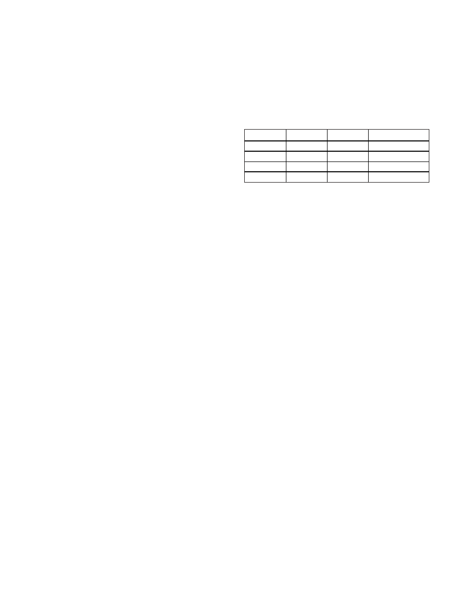
Table 3. Internal Pullup Resistor Control
in Peripheral Mode
CONNECT
VBGATE
VBUS_DET
PULLUP
0
X
Not Connected
1
0
X
Connected
1
0
Not Connected
1
Connected
相关PDF资料 |
PDF描述 |
|---|---|
| MAX3430ESA+T | IC TXRX RS-485 3.3V 8-SOIC |
| MAX3440EASA+ | IC TXRX RS-485 8-SOIC |
| MAX3452EETE+ | IC USB TRANSCEIVER 16-TQFN |
| MAX3456EETE+T | TXRX USB +/-15KV ESD PROT 16TQFN |
| MAX3464ESA+T | IC TXRX RS485/422 8-SOIC |
相关代理商/技术参数 |
参数描述 |
|---|---|
| MAX3421EETJ+ | 功能描述:外围驱动器与原件 - PCI USB Peripheral Controller w/SPI RoHS:否 制造商:PLX Technology 工作电源电压: 最大工作温度: 安装风格:SMD/SMT 封装 / 箱体:FCBGA-1156 封装:Tray |
| MAX3421EETJ+T | 功能描述:外围驱动器与原件 - PCI USB Peripheral Controller w/SPI RoHS:否 制造商:PLX Technology 工作电源电压: 最大工作温度: 安装风格:SMD/SMT 封装 / 箱体:FCBGA-1156 封装:Tray |
| MAX3421EVKIT-1+ | 功能描述:界面开发工具 MAX3421E/20E Eval Kit RoHS:否 制造商:Bourns 产品:Evaluation Boards 类型:RS-485 工具用于评估:ADM3485E 接口类型:RS-485 工作电源电压:3.3 V |
| MAX3430CPA | 功能描述:RS-485接口IC RoHS:否 制造商:Texas Instruments 数据速率:250 Kbps 工作电源电压:3.3 V 电源电流:750 uA 工作温度范围:- 40 C to + 125 C 安装风格:SMD/SMT 封装 / 箱体:SOIC-8 封装:Tube |
| MAX3430CPA+ | 功能描述:RS-485接口IC Fail-Safe 1/4-Unit 3.3V Transceiver RoHS:否 制造商:Texas Instruments 数据速率:250 Kbps 工作电源电压:3.3 V 电源电流:750 uA 工作温度范围:- 40 C to + 125 C 安装风格:SMD/SMT 封装 / 箱体:SOIC-8 封装:Tube |
发布紧急采购,3分钟左右您将得到回复。