- 您现在的位置:买卖IC网 > PDF目录2009 > MAX3886ETN+T (Maxim Integrated Products)IC MULTIRATE CDR SER/DES56-TQFN PDF资料下载
参数资料
| 型号: | MAX3886ETN+T |
| 厂商: | Maxim Integrated Products |
| 文件页数: | 7/17页 |
| 文件大小: | 0K |
| 描述: | IC MULTIRATE CDR SER/DES56-TQFN |
| 标准包装: | 2,500 |
| 类型: | 时钟和数据恢复(CDR),多路复用器 |
| PLL: | 是 |
| 主要目的: | 光纤网络终端(ONT)应用,千兆位无源光纤网络(GPON),宽带无源光纤网络(BPON) |
| 输入: | CML,LVDS,LVPECL |
| 输出: | CML,LVDS |
| 电路数: | 1 |
| 比率 - 输入:输出: | 7:6 |
| 差分 - 输入:输出: | 是/是 |
| 频率 - 最大: | 622MHz,2488Mbps |
| 电源电压: | 3 V ~ 3.6 V |
| 工作温度: | -40°C ~ 85°C |
| 安装类型: | 表面贴装 |
| 封装/外壳: | 56-WFQFN 裸露焊盘 |
| 供应商设备封装: | 56-TQFN-EP(8x8) |
| 包装: | 带卷 (TR) |
MAX3886
Multirate CDR with Integrated Serializer/Deserializer
for GPON and BPON ONT Applications
______________________________________________________________________________________
15
FIFO Control Signals
A valid input at FRST is required to initialize the FIFO
after the relationship between PCKO or RCKO and PCKI
has stabilized prior to operating the serializer, or after the
FERR output has indicated that the FIFO has overflowed
or underflowed due to the phase difference between
PCKO or RCKO and PCKI exceeding its capacity. The
MAC IC provides the control signal for FRST. FERR
should not be directly connected to FRST.
If the PCKI signal is interrupted between bursts, the
FIFO must be reset before the beginning of each burst
while valid clocks are present. If a continuous PCKI sig-
nal is provided between bursts, the FIFO maintains the
correct FIFO counter values as long as the phase rela-
tionship does not change.
Reference Clock Oscillator
The integrated reference oscillator requires a parallel
resonant 19.4400MHz AT-strip cut crystal connected
between pins RFCK1 and RFCK2. It has 18pF nominal
(15pF to 21pF) of on-chip crystal load capacitance; any
frequency error due to mismatch to the rated crystal
load capacitance must be included in the budget for
the difference between reference clock frequency and
input data rate. Take care that the wiring capacitances
at the nodes RFCK1 and RFCK2 are controlled (typical-
ly no more than 2pF) to ensure proper operation.
To drive the reference clock with an external
19.4400MHz LVCMOS clock source, connect it to
RFCK1 through a 10pF ±10% series capacitor and
leave RFCK2 open. The LVCMOS clock source must be
capable of driving a 10pF load.
To ensure proper acquisition, the maximum difference
between the downstream data rate (divided down to
19.4400MHz) and 19.4400MHz clock should be
500ppm, including 57ppm required by the CDR itself.
Table 3 shows a typical budget.
Table 3. Typical Frequency Budget
MAX3886
VCC
MVCO
P
N
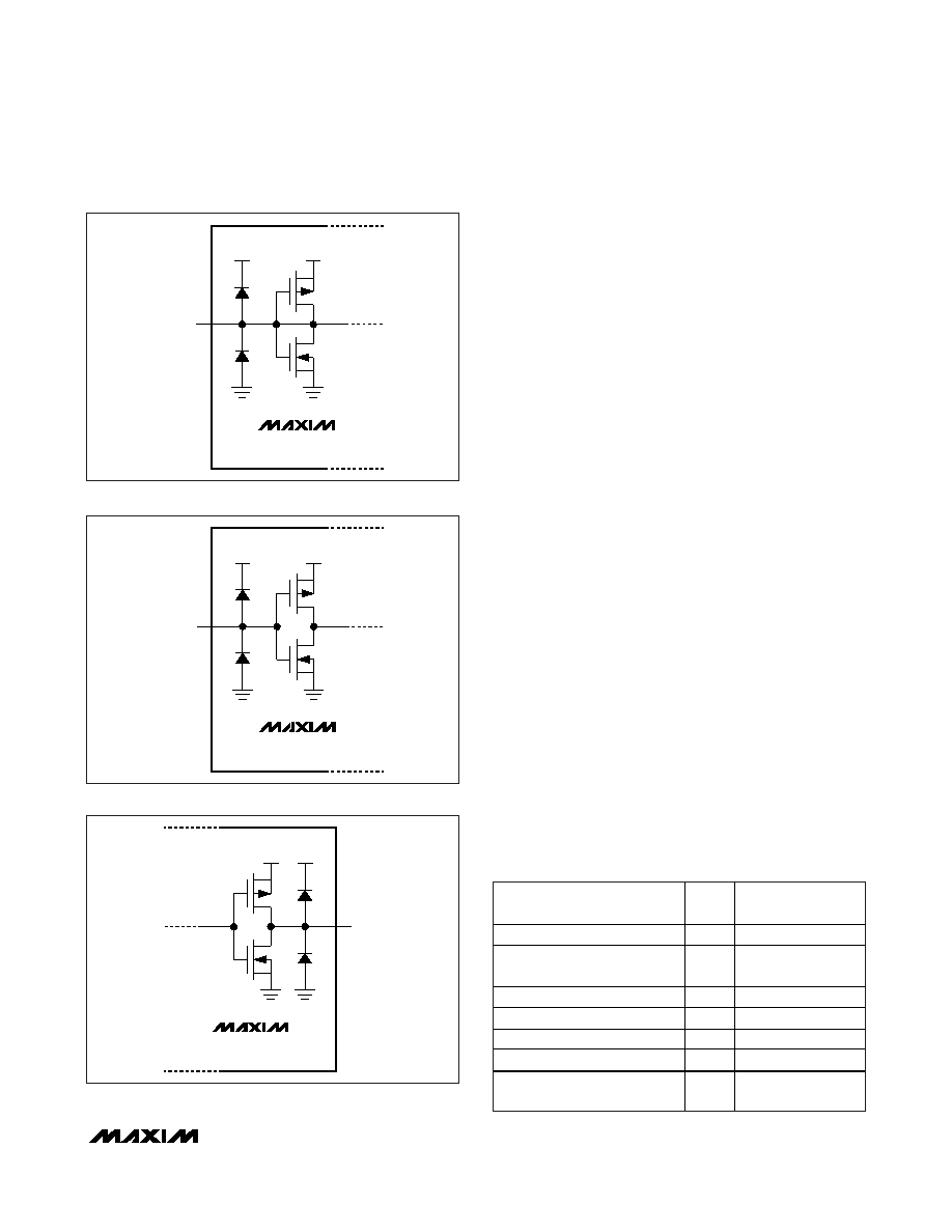
Figure 11. Three-State Input (MVCO)
MAX3886
VCC
MSYM
MDDR
FRST
P
N
Figure 12. LVCMOS Inputs
MAX3886
VCC
LOCK
FERR
P
N
Figure 13. LVCMOS Outputs
DESCRIPTION
f
(±ppm)
NOTES
Downstream Data Rate
50
G.983, G.984
Crystal Load Capacitance
63
e.g., 21ppm/pF
from 18pF
Crystal Tolerance
75
Crystal Temperature Stability
100
Crystal Aging
50
CDR Operation
57
Total
395
Total is less than
500ppm
相关PDF资料 |
PDF描述 |
|---|---|
| MAX3991UTG+T | IC DATA RECOVERY W/AMP 24-TQFN |
| MAX3992UTG+T | IC DATA RECOVERY W/EQ 24-TQFN |
| MAX504EPD+ | IC DAC 10BIT 5V LP SER 14-DIP |
| MAX507AENG+ | IC DAC 12BIT W/REF 24-DIP |
| MAX5100AEUP+T | IC DAC 8BIT QUAD R-R 20TSSOP |
相关代理商/技术参数 |
参数描述 |
|---|---|
| MAX388C/D | 功能描述:多路器开关 IC RoHS:否 制造商:Texas Instruments 通道数量:1 开关数量:4 开启电阻(最大值):7 Ohms 开启时间(最大值): 关闭时间(最大值): 传播延迟时间:0.25 ns 工作电源电压:2.3 V to 3.6 V 工作电源电流: 最大工作温度:+ 85 C 安装风格:SMD/SMT 封装 / 箱体:UQFN-16 |
| MAX388CJN | 功能描述:多路器开关 IC RoHS:否 制造商:Texas Instruments 通道数量:1 开关数量:4 开启电阻(最大值):7 Ohms 开启时间(最大值): 关闭时间(最大值): 传播延迟时间:0.25 ns 工作电源电压:2.3 V to 3.6 V 工作电源电流: 最大工作温度:+ 85 C 安装风格:SMD/SMT 封装 / 箱体:UQFN-16 |
| MAX388CPN | 功能描述:多路器开关 IC RoHS:否 制造商:Texas Instruments 通道数量:1 开关数量:4 开启电阻(最大值):7 Ohms 开启时间(最大值): 关闭时间(最大值): 传播延迟时间:0.25 ns 工作电源电压:2.3 V to 3.6 V 工作电源电流: 最大工作温度:+ 85 C 安装风格:SMD/SMT 封装 / 箱体:UQFN-16 |
| MAX388CPN+ | 功能描述:多路器开关 IC 8:1 8Ch Fault Prtcd Analog MUX RoHS:否 制造商:Texas Instruments 通道数量:1 开关数量:4 开启电阻(最大值):7 Ohms 开启时间(最大值): 关闭时间(最大值): 传播延迟时间:0.25 ns 工作电源电压:2.3 V to 3.6 V 工作电源电流: 最大工作温度:+ 85 C 安装风格:SMD/SMT 封装 / 箱体:UQFN-16 |
| MAX388CWG | 功能描述:多路器开关 IC RoHS:否 制造商:Texas Instruments 通道数量:1 开关数量:4 开启电阻(最大值):7 Ohms 开启时间(最大值): 关闭时间(最大值): 传播延迟时间:0.25 ns 工作电源电压:2.3 V to 3.6 V 工作电源电流: 最大工作温度:+ 85 C 安装风格:SMD/SMT 封装 / 箱体:UQFN-16 |
发布紧急采购,3分钟左右您将得到回复。