参数资料
| 型号: | MAX4019ESD+T |
| 厂商: | Maxim Integrated Products |
| 文件页数: | 12/12页 |
| 文件大小: | 0K |
| 描述: | IC BUFFER R-R 14SOIC |
| 产品培训模块: | Lead (SnPb) Finish for COTS Obsolescence Mitigation Program |
| 标准包装: | 2,500 |
| 放大器类型: | 缓冲器 |
| 电路数: | 3 |
| 输出类型: | 满摆幅 |
| 转换速率: | 600 V/µs |
| -3db带宽: | 200MHz |
| 电流 - 输入偏压: | 5.4µA |
| 电压 - 输入偏移: | 4000µV |
| 电流 - 电源: | 5.5mA |
| 电流 - 输出 / 通道: | 120mA |
| 电压 - 电源,单路/双路(±): | 3.15 V ~ 11 V,±1.575 V ~ 5.5 V |
| 工作温度: | -40°C ~ 85°C |
| 安装类型: | 表面贴装 |
| 封装/外壳: | 14-SOIC(0.154",3.90mm 宽) |
| 供应商设备封装: | 14-SOIC |
| 包装: | 带卷 (TR) |
MAX4014/MAX4017/MAX4019/MAX4022
Low-Cost, High-Speed, Single-Supply, Gain of +2
Buffers with Rail-to-Rail Outputs in SOT23
_______________________________________________________________________________________
9
Input Voltage Range and Output Swing
The input range for the MAX4014 family extends from
(VEE - 100mV) to (VCC - 2.25V). Input ground sensing
increases the dynamic range for single-supply applica-
tions. The outputs drive a 2k
load to within 60mV of
the power-suply rails. With heavier loads, the output
swing is reduced as shown in the Electrical Character-
istics and the Typical Operating Characteristics. As the
load increases, the input range is effectively limited by
the output-drive capability, since the buffers have a
fixed voltage gain of +2 or -1.
For example, a 50
load can typically be driven from
40mV above VEE to 1.6V below VCC, or 40mV to 3.4V
when operating from a single +5V supply. If the buffer is
operated in the noninverting, gain of +2 configuration
with the inverting input grounded, the effective input
voltage range becomes 20mV to 1.7V, instead of the
-100mV to 2.75V indicated by the Electrical Character-
istics. Beyond the effective input range, the buffer out-
put is a nonlinear function of the input, but it will not
undergo phase reversal or latchup.
Enable
The MAX4019 has an enable feature (EN_) that allows
the buffer to be placed in a low-power state. When the
buffers are disabled, the supply current will not exceed
550A per buffer.
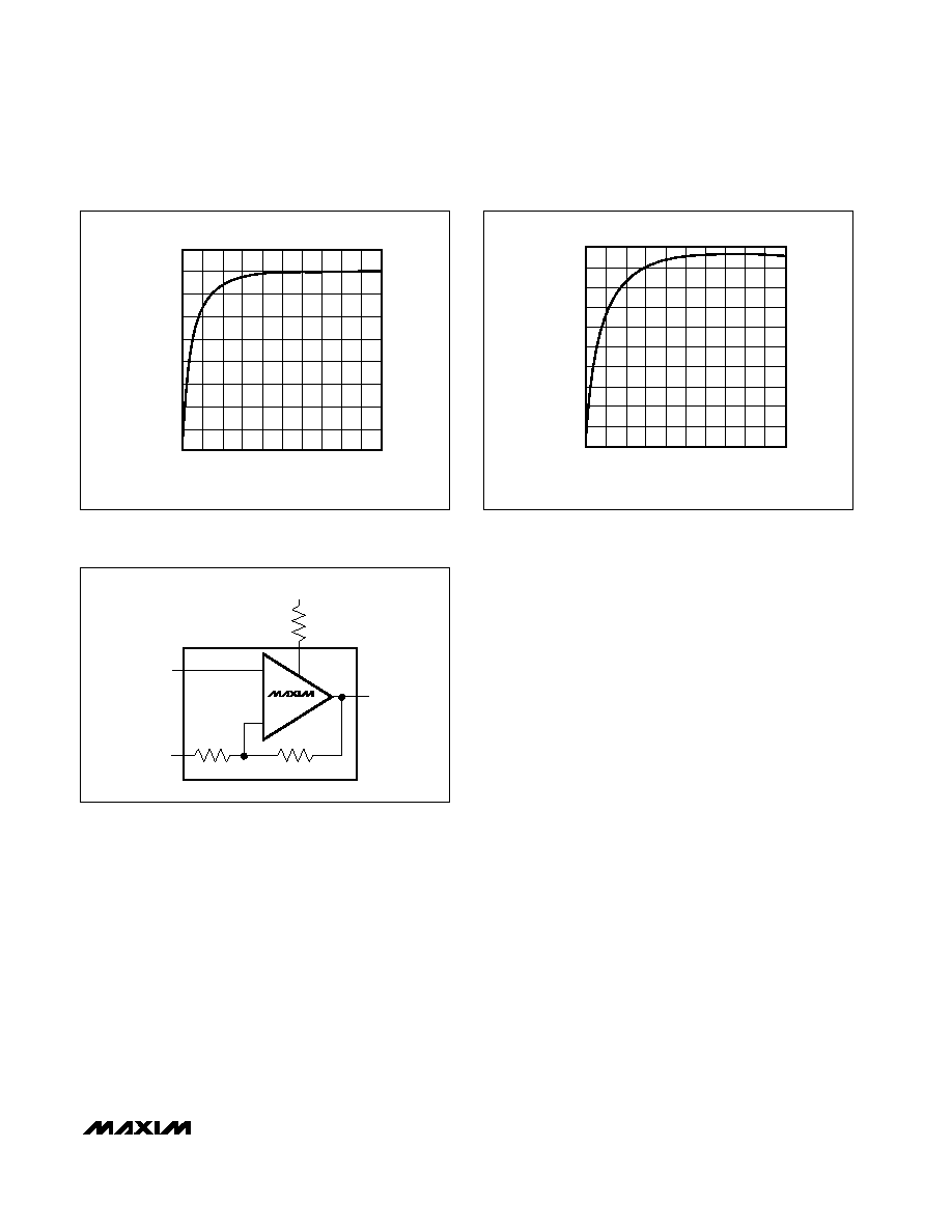
As the voltage at the EN_ pin approaches the negative
supply rail, the EN_ input current rises. Figure 2 shows
a graph of EN_ input current versus EN_ pin voltage.
Figure 3 shows the addition of an optional resistor in
series with the EN pin, to limit the magnitude of the cur-
rent increase. Figure 4 displays the resulting EN pin
input current to voltage relationship.
20
-160
0
100
300
500
-100
-120
0
VIL (mV ABOVE VEE)
INPUT
CURRENT
(
A)
200
400
-60
-140
-20
-40
-80
Figure 2. Enable Logic-Low Input Current vs. Enable Logic-
Low Threshold
OUT
IN-
EN_
IN+
10k
ENABLE
MAX40_ _
500
500
Figure 3. Circuit to Reduce Enable Logic-Low Input Current
0
-10
0
100
300
500
-7
-8
-1
VIL (mV ABOVE VEE)
INPUT
CURRENT
(
A)
200
400
-3
-5
-9
-2
-4
-6
Figure 4. Enable Logic-Low Input Current vs. Enable Logic-
Low Threshold with 10k
Series Resistor
相关PDF资料 |
PDF描述 |
|---|---|
| 324955 | CONN RING 14-16 AWG #8 SOLIS |
| 36150 | CONN RING 16-22 AWG #6 PIDG |
| 796590-9 | 25P ACT PIN,MMATE LF |
| 51864 | CONN RING 14-16 AWG #6 PIDG |
| MAX4019EEE+T | IC BUFFER R-R 16QSOP |
相关代理商/技术参数 |
参数描述 |
|---|---|
| MAX4020 | 制造商:MAXIM 制造商全称:Maxim Integrated Products 功能描述:Low-Cost, High-Speed, SOT23, Single-Supply Op Amps with Rail-to-Rail Outputs |
| MAX40-20.0C | 制造商:MDE 制造商全称:MDE Semiconductor, Inc. 功能描述:HIGH CURRENT TRANSIENT VOLTAGE SUPPRESSOR (TVS) DIODE |
| MAX40-20.0CA | 制造商:MDE 制造商全称:MDE Semiconductor, Inc. 功能描述:HIGH CURRENT TRANSIENT VOLTAGE SUPPRESSOR (TVS) DIODE |
| MAX40-20CA | 制造商:MDE 制造商全称:MDE Semiconductor, Inc. 功能描述:HIGH CURRENT TRANSIENT VOLTAGE SUPPRESSOR (TVS) DIODE STAND-OFF VOLTAGE 12 TO 150 Volts 40000 Watt Peak Pulse Power |
| MAX4020EEE | 功能描述:高速运算放大器 RoHS:否 制造商:Texas Instruments 通道数量:1 电压增益 dB:116 dB 输入补偿电压:0.5 mV 转换速度:55 V/us 工作电源电压:36 V 电源电流:7.5 mA 最大工作温度:+ 85 C 安装风格:SMD/SMT 封装 / 箱体:SOIC-8 封装:Tube |
发布紧急采购,3分钟左右您将得到回复。