参数资料
| 型号: | MAX4019ESD+T |
| 厂商: | Maxim Integrated Products |
| 文件页数: | 5/12页 |
| 文件大小: | 0K |
| 描述: | IC BUFFER R-R 14SOIC |
| 产品培训模块: | Lead (SnPb) Finish for COTS Obsolescence Mitigation Program |
| 标准包装: | 2,500 |
| 放大器类型: | 缓冲器 |
| 电路数: | 3 |
| 输出类型: | 满摆幅 |
| 转换速率: | 600 V/µs |
| -3db带宽: | 200MHz |
| 电流 - 输入偏压: | 5.4µA |
| 电压 - 输入偏移: | 4000µV |
| 电流 - 电源: | 5.5mA |
| 电流 - 输出 / 通道: | 120mA |
| 电压 - 电源,单路/双路(±): | 3.15 V ~ 11 V,±1.575 V ~ 5.5 V |
| 工作温度: | -40°C ~ 85°C |
| 安装类型: | 表面贴装 |
| 封装/外壳: | 14-SOIC(0.154",3.90mm 宽) |
| 供应商设备封装: | 14-SOIC |
| 包装: | 带卷 (TR) |
mA
MAX4014/MAX4017/MAX4019/MAX4022
Low-Cost, High-Speed, Single-Supply, Gain of +2
Buffers with Rail-to-Rail Outputs in SOT23
2
_______________________________________________________________________________________
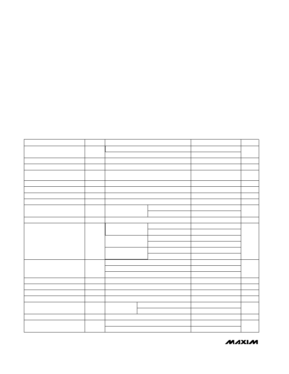
ABSOLUTE MAXIMUM RATINGS
DC ELECTRICAL CHARACTERISTICS
(VCC = +5V, VEE = 0V, IN_- =0V, EN_ = 5V, RL =
∞ to ground, VOUT = VCC / 2, noninverting configuration, TA = TMIN to TMAX, unless
otherwise noted. Typical values are at TA = +25°C.) (Note 1)
Supply Voltage (VCC to VEE) ..................................................12V
IN_-, IN_+, OUT_, EN_ ....................(VEE - 0.3V) to (VCC + 0.3V)
Output Short-Circuit Duration to VCC or VEE ..............Continuous
Continuous Power Dissipation (TA = +70°C)
5-pin SOT23 (derate 7.1mW/°C above+70°C)..............571mW
8-pin SO (derate 5.9mW/°C above +70°C)...................471mW
8-pin MAX (derate 4.1mW/°C above +70°C) ..............330mW
14-pin SO (derate 8.3mW/°C above +70°C).................667mW
16-pin QSOP (derate 8.3mW/°C above +70°C)............667mW
Operating Temperature Range ...........................-40°C to +85°C
Storage Temperature Range .............................-65°C to +150°C
Lead Temperature (soldering, 10sec) .............................+300°C
Stresses beyond those listed under “Absolute Maximum Ratings” may cause permanent damage to the device. These are stress ratings only, and functional
operation of the device at these or at any other conditions beyond those indicated in the operational sections of the specifications is not implied. Exposure
to absolute maximum rating conditions for extended periods may affect device reliability.
V
EN_ Logic-High Threshold
VIH
MAX4019
VCC - 1.5
V
EN_ Logic-Low Threshold
VIL
MAX4019
VCC - 2.6
k
Disabled Output Resistance
ROUT(OFF) MAX4019, EN_ = 0V, 0V
≤ VOUT ≤ 5V
1
V
Operating Supply-Voltage Range
VCC to VEE
3.15
11.0
dB
Power-Supply Rejection Ratio
(Note 3)
PSRR
VCC = 5V, VEE = 0V, VOUT = 2V
46
57
Output Current
IOUT
±70
±120
mA
RL = 20
to VCC or
VEE
Output Resistance
ROUT
25
m
f = DC
Short-Circuit Output Current
ISC
±150
mA
Sinking or sourcing
VEE - 0.1
VCC + 0.1
IN_-
VOL - VEE
VCC - VOH
VOL - VEE
VCC - VOH
VOL - VEE
VCC - VOH
0.06
RL = 2k
0.04
0.50
0.75
1.50
RL =150
0.04
0.50
Output Voltage Swing
VOUT
V
1.60
2.00
RL = 50
PARAMETER
SYMBOL
MIN
TYP
MAX
UNITS
Input Resistance
RIN
3
M
Input Bias Current
IB
5.4
20
A
Input Offset Voltage Matching
±1
mV
Voltage Gain
AV
1.9
2
2.1
V/V
Input Offset Voltage
Input Voltage Range
VIN
VEE - 0.1
VCC - 2.25
V
VOS
420
mV
Input Offset Voltage Drift
TCVOS
8
V/°C
CONDITIONS
IN_+, over input voltage range
IN_+ (Note 2)
Any channels for
MAX4017/MAX4019/MAX4022
RL
≥ 50, (VEE + 0.5V) ≤ VOUT ≤ (VCC - 2.0V)
IN_+
RL = 50
A
EN_ Logic Input Low Current
IIL
0.5
VCC = 5V, VEE = -5V, VOUT = 0V
54
66
VCC = 3.3V, VEE = 0V, VOUT = 0.9V
45
MAX4019
(VEE + 0.2V)
≤ EN_ ≤ VCC
200
550
EN_ = VEE
A
EN_ Logic Input High Current
IIH
0.5
10
MAX4019, EN_ = VCC
mA
Quiescent Supply Current
(per Buffer)
ICC
5.5
8.0
Enabled (EN_ = VCC)
0.4
0.7
MAX4019, disabled (EN_ = VEE)
±60
TA = +25°C
TA = TMIN to TMAX
相关PDF资料 |
PDF描述 |
|---|---|
| 324955 | CONN RING 14-16 AWG #8 SOLIS |
| 36150 | CONN RING 16-22 AWG #6 PIDG |
| 796590-9 | 25P ACT PIN,MMATE LF |
| 51864 | CONN RING 14-16 AWG #6 PIDG |
| MAX4019EEE+T | IC BUFFER R-R 16QSOP |
相关代理商/技术参数 |
参数描述 |
|---|---|
| MAX4020 | 制造商:MAXIM 制造商全称:Maxim Integrated Products 功能描述:Low-Cost, High-Speed, SOT23, Single-Supply Op Amps with Rail-to-Rail Outputs |
| MAX40-20.0C | 制造商:MDE 制造商全称:MDE Semiconductor, Inc. 功能描述:HIGH CURRENT TRANSIENT VOLTAGE SUPPRESSOR (TVS) DIODE |
| MAX40-20.0CA | 制造商:MDE 制造商全称:MDE Semiconductor, Inc. 功能描述:HIGH CURRENT TRANSIENT VOLTAGE SUPPRESSOR (TVS) DIODE |
| MAX40-20CA | 制造商:MDE 制造商全称:MDE Semiconductor, Inc. 功能描述:HIGH CURRENT TRANSIENT VOLTAGE SUPPRESSOR (TVS) DIODE STAND-OFF VOLTAGE 12 TO 150 Volts 40000 Watt Peak Pulse Power |
| MAX4020EEE | 功能描述:高速运算放大器 RoHS:否 制造商:Texas Instruments 通道数量:1 电压增益 dB:116 dB 输入补偿电压:0.5 mV 转换速度:55 V/us 工作电源电压:36 V 电源电流:7.5 mA 最大工作温度:+ 85 C 安装风格:SMD/SMT 封装 / 箱体:SOIC-8 封装:Tube |
发布紧急采购,3分钟左右您将得到回复。