- 您现在的位置:买卖IC网 > PDF目录14390 > MAX630CSA+ (Maxim Integrated Products)IC REG BOOST 0.15A 8SOIC PDF资料下载
参数资料
| 型号: | MAX630CSA+ |
| 厂商: | Maxim Integrated Products |
| 文件页数: | 4/14页 |
| 文件大小: | 0K |
| 描述: | IC REG BOOST 0.15A 8SOIC |
| 产品培训模块: | Lead (SnPb) Finish for COTS Obsolescence Mitigation Program |
| 标准包装: | 100 |
| 类型: | 升压(升压) |
| 输出数: | 1 |
| 输入电压: | 2 V ~ 16.5 V |
| 频率 - 开关: | 40kHz |
| 电流 - 输出: | 150mA |
| 同步整流器: | 无 |
| 工作温度: | 0°C ~ 70°C |
| 安装类型: | 表面贴装 |
| 封装/外壳: | 8-SOIC(0.154",3.90mm 宽) |
| 包装: | 管件 |
| 供应商设备封装: | 8-SOIC |
�� �
�
�CMOS� Micropower� Step-Up�
�Switching� Regulator�
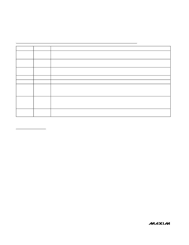
�Pin� Description�
�PIN�
�1�
�2�
�3�
�4�
�5�
�6�
�7�
�8�
�NAME�
�LBR�
�C� X�
�L� X�
�GND�
�+V� S�
�I� C�
�V� FB�
�LBD�
�FUNCTION�
�Low-Battery� Detection� Comparator� Input.� The� LBD� output,� pin� 8,� sinks� current� whenever� this� pin� is�
�below� the� low-battery� detector� threshold,� typically� 1.31V.�
�An� external� capacitor� connected� between� this� terminal� and� ground� sets� the� oscillator� frequency.�
�47pF� =� 40� kHz.�
�This� pin� drives� the� external� inductor.� The� internal� N-channel� MOSFET� that� drives� L� X� has� an� output�
�resistance� of� 4� Ω� and� a� peak� current� rating� of� 525mA.�
�Ground�
�The� positive� supply� voltage,� from� 2.0V� to� 16.5V� (MAX630).�
�The� MAX630/MAX4193� shut� down� when� this� pin� is� left� floating� or� is� driven� below� 0.2V.� For� normal�
�operation,� connect� I� C� directly� to� +V� S� or� drive� it� high� with� either� a� CMOS� gate� or� pullup� resistor�
�connected� to� +V� S� .� The� supply� current� is� typically� 10nA� in� the� shutdown� mode�
�The� output� voltage� is� set� by� an� external� resistive� divider� connected� from� the� converter� output� to� V� FB�
�and� ground.� The� MAX630/MAX4193� pulse� the� L� X� output� whenever� the� voltage� at� this� terminal� is� less�
�than� 1.31V.�
�The� Low-Battery� Detector� output� is� an� open-drain� N-channel� MOSFET� that� sinks� up� to� 600� μ� A� (typ)�
�whenever� the� LBR� input,� pin� 1,� is� below� 1.31V.�
�Detailed� Description�
�The� operation� of� the� MAX630� can� best� be� understood�
�by� examining� the� voltage� regulating� loop� of� Figure� 1.�
�R1� and� R2� divide� the� output� voltage,� which� is� com-�
�pared� with� the� 1.3V� internal� reference� by� comparator�
�COMP1.� When� the� output� voltage� is� lower� than� desired,�
�the� comparator� output� goes� high� and� the� oscillator� out-�
�put� pulses� are� passed� through� the� NOR� gate� latch,�
�turning� on� the� output� N-channel� MOSFET� at� pin� 3,� L� X� .�
�As� long� as� the� output� voltage� is� less� than� the� desired�
�voltage,� pin� 3� drives� the� inductor� with� a� series� of� pulses�
�at� the� oscillator� frequency.�
�Each� time� the� output� N-channel� MOSFET� is� turned� on,�
�the� current� through� the� external� coil,� L1,� increases,�
�storing� energy� in� the� coil.� Each� time� the� output� turns� off,�
�the� voltage� across� the� coil� reverses� sign� and� the� volt-�
�age� at� L� X� rises� until� the� catch� diode,� D1,� is� forward�
�biased,� delivering� power� to� the� output.�
�When� the� output� voltage� reaches� the� desired� level,�
�1.31V� x� (1� +� R1� /� R2),� the� comparator� output� goes� low�
�and� the� inductor� is� no� longer� pulsed.� Current� is� then�
�supplied� by� the� filter� capacitor,� C1,� until� the� output� volt-�
�age� drops� below� the� threshold,� and� once� again� L� X� is�
�switched� on,� repeating� the� cycle.� The� average� duty�
�cycle� at� L� X� is� directly� proportional� to� the� output� current.�
�Output� Driver� (L� X� Pin)�
�The� MAX630/MAX4193� output� device� is� a� large�
�N-channel� MOSFET� with� an� on-resistance� of� 4� Ω� and� a�
�peak� current� rating� of� 525mA.� One� well-known� advan-�
�tage� that� MOSFETs� have� over� bipolar� transistors� in�
�switching� applications� is� higher� speed,� which� reduces�
�switching� losses� and� allows� the� use� of� smaller,� lighter,�
�less� costly� magnetic� components.� Also� important� is� that�
�MOSFETs,� unlike� bipolar� transistors,� do� not� require�
�base� current� that,� in� low-power� DC-DC� converters,�
�often� accounts� for� a� major� portion� of� input� power.�
�The� operating� current� of� the� MAX630� and� MAX4193�
�increases� by� approximately� 1μA/kHz� at� maximum�
�power� output� due� to� the� charging� current� required� by�
�the� gate� capacitance� of� the� L� X� output� driver� (e.g.,� 40μA�
�increase� at� a� 40kHz� operating� frequency).� In� compari-�
�son,� equivalent� bipolar� circuits� typically� drive� their� NPN�
�L� X� output� device� with� 2mA� of� base� drive,� causing� the�
�bipolar� circuit’s� operating� current� to� increase� by� a� fac-�
�tor� of� 10� between� no� load� and� full� load.�
�Oscillator�
�The� oscillator� frequency� is� set� by� a� single� external,� low-�
�cost� ceramic� capacitor� connected� to� pin� 2,� C� X� .� 47pF�
�sets� the� oscillator� to� 40kHz,� a� reasonable� compromise�
�between� lower� switching� losses� at� low� frequencies� and�
�reduced� inductor� size� at� higher� frequencies.�
�4�
�_______________________________________________________________________________________�
�相关PDF资料 |
PDF描述 |
|---|---|
| MAX634CSA+ | IC REG INV FLYBK ADJ 0.15A 8SOIC |
| ECC43DRXI | CONN EDGECARD 86POS DIP .100 SLD |
| RCM28DRYH | CONN EDGECARD 56POS DIP .156 SLD |
| ESC22DRAN | CONN EDGECARD 44POS R/A .100 SLD |
| LQW15AN4N1B00D | INDUCTOR |
相关代理商/技术参数 |
参数描述 |
|---|---|
| MAX630CSA+ | 功能描述:直流/直流开关调节器 CMOS uPower Step Up Switching Reg RoHS:否 制造商:International Rectifier 最大输入电压:21 V 开关频率:1.5 MHz 输出电压:0.5 V to 0.86 V 输出电流:4 A 输出端数量: 最大工作温度: 安装风格:SMD/SMT 封装 / 箱体:PQFN 4 x 5 |
| MAX630CSA+T | 功能描述:直流/直流开关调节器 CMOS uPower Step Up Switching Reg RoHS:否 制造商:International Rectifier 最大输入电压:21 V 开关频率:1.5 MHz 输出电压:0.5 V to 0.86 V 输出电流:4 A 输出端数量: 最大工作温度: 安装风格:SMD/SMT 封装 / 箱体:PQFN 4 x 5 |
| MAX630CSA-C70048 | 制造商:Rochester Electronics LLC 功能描述: 制造商:Maxim Integrated Products 功能描述: |
| MAX630CSA-C71098 | 制造商:Maxim Integrated Products 功能描述:8 PINS N.SO PKG - Rail/Tube |
| MAX630CSA-T | 功能描述:直流/直流开关调节器 CMOS uPower Step Up Switching Reg RoHS:否 制造商:International Rectifier 最大输入电压:21 V 开关频率:1.5 MHz 输出电压:0.5 V to 0.86 V 输出电流:4 A 输出端数量: 最大工作温度: 安装风格:SMD/SMT 封装 / 箱体:PQFN 4 x 5 |
发布紧急采购,3分钟左右您将得到回复。