- 您现在的位置:买卖IC网 > PDF目录14390 > MAX630CSA+ (Maxim Integrated Products)IC REG BOOST 0.15A 8SOIC PDF资料下载
参数资料
| 型号: | MAX630CSA+ |
| 厂商: | Maxim Integrated Products |
| 文件页数: | 5/14页 |
| 文件大小: | 0K |
| 描述: | IC REG BOOST 0.15A 8SOIC |
| 产品培训模块: | Lead (SnPb) Finish for COTS Obsolescence Mitigation Program |
| 标准包装: | 100 |
| 类型: | 升压(升压) |
| 输出数: | 1 |
| 输入电压: | 2 V ~ 16.5 V |
| 频率 - 开关: | 40kHz |
| 电流 - 输出: | 150mA |
| 同步整流器: | 无 |
| 工作温度: | 0°C ~ 70°C |
| 安装类型: | 表面贴装 |
| 封装/外壳: | 8-SOIC(0.154",3.90mm 宽) |
| 包装: | 管件 |
| 供应商设备封装: | 8-SOIC |
�� �
�
�CMOS� Micropower� Step-Up�
�Switching� Regulator�
�LOW� BATTERY� INPUT�
�+5V� INPUT�
�L1�
�R3�
�169k� Ω�
�1� LBR�
�R4�
�100k� Ω�
�1.31V�
�COMP� 2�
�MAX630�
�LBD� 8�
�LOW-BATTERY� OUTPUT�
�(LOW� IF� INPUT� <� 3V)�
�470�
�R2�
�2� C� X�
�3� L� X�
�OSC�
�40kHz�
�COMP� 1�
�V� FB� 7�
�I� C� 6�
�C� C�
�47.5k� Ω�
�R1�
�499k� Ω�
�SHUTDOWN�
�D1�
�1N4148�
�R� ON� ?� 3� Ω�
�4� GND�
�1.31V�
�BANDGAP�
�REFERENCE�
�AND�
�+V� S� 5�
�OPERATE�
�BIAS� GENERATOR�
�+15V� OUTPUT�
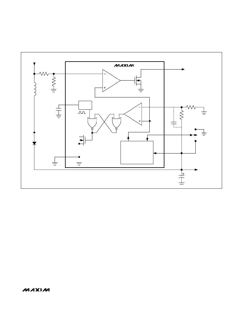
�Figure� 1.� +5V� to� +15V� Converter� and� Block� Diagram�
�C1�
�470� μ� F�
�25V�
�20mA�
�Low-Battery� Detector�
�The� low-battery� detector� compares� the� voltage� on� LBR�
�with� the� internal� 1.31V� reference.� The� output,� LBD,� is� an�
�open-drain� N-channel� MOSFET.� In� addition� to� detecting�
�and� warning� of� a� low� battery� voltage,� the� comparator�
�can� also� perform� other� voltage-monitoring� operations�
�such� as� power-failure� detection.�
�Another� use� of� the� low-battery� detector� is� to� lower� the�
�oscillator� frequency� when� the� input� voltage� goes� below�
�a� specified� level.� Lowering� the� oscillator� frequency�
�increases� the� available� output� power,� compensating� for�
�the� decrease� in� available� power� caused� by� reduced�
�input� voltage� (see� Figure� 5).�
�Logic-Level� Shutdown� Input�
�The� shutdown� mode� is� entered� whenever� I� C� (pin� 6)� is�
�driven� below� 0.2V� or� left� floating.� When� shut� down,� the�
�MAX630’s� analog� circuitry,� oscillator,� L� X� ,� and� LBD� out-�
�puts� are� turned� off.� The� device’s� quiescent� current� dur-�
�ing� shutdown� is� typically� 10nA� (1μA� max).�
�Bootstrapped� Operation�
�In� most� circuits,� the� preferred� source� of� +V� S� voltage� for�
�the� MAX630� and� MAX4193� is� the� boosted� output� volt-�
�age.� This� is� often� referred� to� as� a� “bootstrapped”� oper-�
�ation� since� the� circuit� figuratively� “lifts”� itself� up.�
�The� on-resistance� of� the� N-channel� L� X� output� decreas-�
�es� with� an� increase� in� +V� S� ;� however,� the� device� operat-�
�ing� current� goes� up� with� +V� S� (see� the� Typical�
�Operating� Characteristics� ,� I� S� vs.� +V� S� graph).� In� circuits�
�with� very� low� output� current� and� input� voltages� greater�
�than� 3V,� it� may� be� more� efficient� to� connect� +V� S� direct-�
�ly� to� the� input� voltage� rather� than� bootstrap.�
�_______________________________________________________________________________________�
�5�
�相关PDF资料 |
PDF描述 |
|---|---|
| MAX634CSA+ | IC REG INV FLYBK ADJ 0.15A 8SOIC |
| ECC43DRXI | CONN EDGECARD 86POS DIP .100 SLD |
| RCM28DRYH | CONN EDGECARD 56POS DIP .156 SLD |
| ESC22DRAN | CONN EDGECARD 44POS R/A .100 SLD |
| LQW15AN4N1B00D | INDUCTOR |
相关代理商/技术参数 |
参数描述 |
|---|---|
| MAX630CSA+ | 功能描述:直流/直流开关调节器 CMOS uPower Step Up Switching Reg RoHS:否 制造商:International Rectifier 最大输入电压:21 V 开关频率:1.5 MHz 输出电压:0.5 V to 0.86 V 输出电流:4 A 输出端数量: 最大工作温度: 安装风格:SMD/SMT 封装 / 箱体:PQFN 4 x 5 |
| MAX630CSA+T | 功能描述:直流/直流开关调节器 CMOS uPower Step Up Switching Reg RoHS:否 制造商:International Rectifier 最大输入电压:21 V 开关频率:1.5 MHz 输出电压:0.5 V to 0.86 V 输出电流:4 A 输出端数量: 最大工作温度: 安装风格:SMD/SMT 封装 / 箱体:PQFN 4 x 5 |
| MAX630CSA-C70048 | 制造商:Rochester Electronics LLC 功能描述: 制造商:Maxim Integrated Products 功能描述: |
| MAX630CSA-C71098 | 制造商:Maxim Integrated Products 功能描述:8 PINS N.SO PKG - Rail/Tube |
| MAX630CSA-T | 功能描述:直流/直流开关调节器 CMOS uPower Step Up Switching Reg RoHS:否 制造商:International Rectifier 最大输入电压:21 V 开关频率:1.5 MHz 输出电压:0.5 V to 0.86 V 输出电流:4 A 输出端数量: 最大工作温度: 安装风格:SMD/SMT 封装 / 箱体:PQFN 4 x 5 |
发布紧急采购,3分钟左右您将得到回复。