- 您现在的位置:买卖IC网 > PDF目录3766 > MAX7314AEG+T (Maxim Integrated Products)IC I/O EXPANDER I2C 16B 24QSOP PDF资料下载
参数资料
| 型号: | MAX7314AEG+T |
| 厂商: | Maxim Integrated Products |
| 文件页数: | 22/25页 |
| 文件大小: | 0K |
| 描述: | IC I/O EXPANDER I2C 16B 24QSOP |
| 产品培训模块: | Lead (SnPb) Finish for COTS Obsolescence Mitigation Program |
| 标准包装: | 2,500 |
| 接口: | I²C |
| 输入/输出数: | 18 |
| 中断输出: | 是 |
| 频率 - 时钟: | 400kHz |
| 电源电压: | 2 V ~ 3.6 V |
| 工作温度: | -40°C ~ 125°C |
| 安装类型: | 表面贴装 |
| 封装/外壳: | 24-SSOP(0.154",3.90mm 宽) |
| 供应商设备封装: | 24-QSOP |
| 包装: | 带卷 (TR) |
MAX7314
Functional Overview
The MAX7314 is a general-purpose input/output (GPIO)
peripheral that provides 16 I/O ports, P0–P15, con-
trolled through an I2C-compatible serial interface. A
17th output-only port, INT/O16, can be configured as
an interrupt output or as a general-purpose output port.
All output ports sink loads up to 50mA connected to
external supplies up to 5.5V, independent of the
MAX7314’s supply voltage. The MAX7314 is rated for a
ground current of 350mA, allowing all 17 outputs to sink
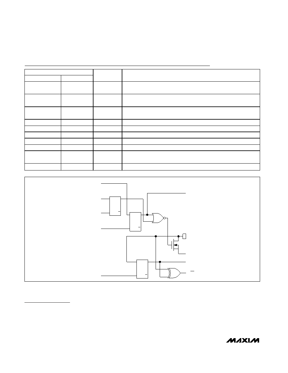
20mA at the same time. Figure 1 shows the output
structure of the MAX7314. The ports default to inputs on
power-up.
18-Port GPIO with LED Intensity Control,
Interrupt, and Hot-Insertion Protection
6
_______________________________________________________________________________________
Pin Description
Figure 1. Simplified Schematic of I/O Ports
D
CK
Q
FF
DATA FROM
SHIFT REGISTER
DATA FROM
SHIFT REGISTER
WRITE
CONFIGURATION
PULSE
WRITE PULSE
READ PULSE
CONFIGURATION
REGISTER
D
CK
Q
FF
INPUT PORT
REGISTER
D
CK
Q
FF
OUTPUT
PORT
REGISTER
OUTPUT PORT
REGISTER DATA
I/O PIN
Q2
GND
INPUT PORT
REGISTER DATA
TO INT
PIN
QSOP
QFN
NAME
FUNCTION
122
INT/O16
Output Port. Open-drain output rated at 7V, 50mA. Configurable as interrupt
output or general-purpose output.
223
RST
Reset Input. Active low clears the 2-wire interface and puts the device in the
same condition as power-up reset.
3
24
AD0
Address Input. Sets device slave address. Connect to either GND, V+, SCL,
or SDA to give four logic combinations. See Table 1.
4–11, 13–20
1–8, 10–17
P0–P15
Input/Output Ports. P0–P15 are open-drain I/Os rated at 5.5V, 50mA.
12
9
GND
Ground. Do not sink more than 350mA into the GND pin.
21
18
BLINK
Input Port Configurable as Blink Control or General-Purpose Input
22
19
SCL
I2C-Compatible Serial Clock Input
23
20
SDA
I2C-Compatible Serial Data I/O
24
21
V+
Positive Supply Voltage. Bypass V+ to GND with a 0.047F ceramic
capacitor.
—
PAD
Exposed Pad
Exposed Pad on Package Underside. Connect to GND.
相关PDF资料 |
PDF描述 |
|---|---|
| ST16C550IQ48-F | IC UART FIFO 16B SGL 48TQFP |
| MAX7318AWG+T | IC PORT EXPANDER 16BIT 24SOIC |
| XR20M1170IL24-F | IC UART FIFO I2C/SPI 64B 24QFN |
| MAX7318AAG+T | IC I/O EXPANDER I2C 16B 24SSOP |
| MAX7318AUG+T | IC I/O EXPANDER I2C 16B 24TSSOP |
相关代理商/技术参数 |
参数描述 |
|---|---|
| MAX7314ATG | 功能描述:外围驱动器与原件 - PCI RoHS:否 制造商:PLX Technology 工作电源电压: 最大工作温度: 安装风格:SMD/SMT 封装 / 箱体:FCBGA-1156 封装:Tray |
| MAX7314ATG+ | 功能描述:外围驱动器与原件 - PCI 18-Port GPIO RoHS:否 制造商:PLX Technology 工作电源电压: 最大工作温度: 安装风格:SMD/SMT 封装 / 箱体:FCBGA-1156 封装:Tray |
| MAX7314ATG+T | 功能描述:接口-I/O扩展器 18-Port GPIO RoHS:否 制造商:NXP Semiconductors 逻辑系列: 输入/输出端数量: 最大工作频率:100 kHz 工作电源电压:1.65 V to 5.5 V 工作温度范围:- 40 C to + 85 C 安装风格:SMD/SMT 封装 / 箱体:HVQFN-16 封装:Reel |
| MAX7314ATG-T | 功能描述:外围驱动器与原件 - PCI RoHS:否 制造商:PLX Technology 工作电源电压: 最大工作温度: 安装风格:SMD/SMT 封装 / 箱体:FCBGA-1156 封装:Tray |
| MAX7314EVKIT+ | 功能描述:外围驱动器与原件 - PCI Evaluation Kit for the MAX7314 RoHS:否 制造商:PLX Technology 工作电源电压: 最大工作温度: 安装风格:SMD/SMT 封装 / 箱体:FCBGA-1156 封装:Tray |
发布紧急采购,3分钟左右您将得到回复。